Merging CPUs and GPUs
AMD has already outlined the beginning of its CPU/GPU merger strategy in a little product called Fusion. While quite bullish on Fusion, AMD hasn't done a tremendous job of truly explaining the importance of Fusion. Fusion, if you haven't heard, is AMD's first single chip CPU/GPU solution due out sometime in the 2008 - 2009 timeframe. Widely expected to be two individual die on a single package, the first incarnation of Fusion will simply be a more power efficient version of a platform with integrated graphics. Integrated graphics is nothing to get excited about, but it is what follows as manufacturing technology and processor architectures evolve that is really interesting.
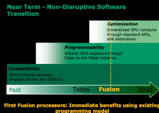
AMD views the Fusion progression as three discrete steps:
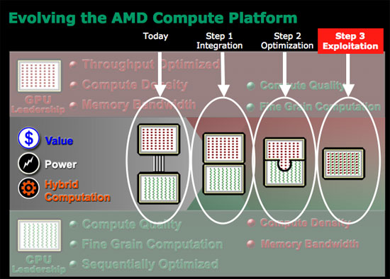
Today we have a CPU and a GPU separated by an external bus, with the two being quite independent. The CPU does what it does best, and the GPU helps out wherever it can. Step 1, is what AMD is calling integration, and it is what we can expect in the first Fusion product due out in 2008 - 2009. The CPU and GPU are simply placed next to one another and there's minor leverage of that relationship, mostly from a cost and power efficiency standpoint.
Step 2, which AMD calls optimization, gets a bit more interesting. Parts of the CPU can be shared by the GPU and vice versa. There's not a deep level of integration, but it begins the transition to the most important step - exploitation.
The final step in the evolution of Fusion is where the CPU and GPU are truly integrated, and the GPU is accessed by user mode instructions just like the CPU. You can expect to talk to the GPU via extensions to the x86 ISA, and the GPU will have its own register file (much like FP and integer units each have their own register files). Elements of the architecture will be shared, especially things like the cache hierarchy, which will prove useful when running applications that require both CPU and GPU power.
The GPU could easily be integrated onto a single die as a separate core behind a shared L3 cache. For example, if you look at the current Barcelona architecture you have four homogenous cores behind a shared L3 cache and memory controller; simply swap one of those cores with a GPU core and you've got an idea of what one of these chips could look like. Instructions that can only be processed by the specialized core will be dispatched directly to it, while instructions better suited for other cores will be sent to them. There would have to be a bit of front end logic to manage all of this, but it's easily done.
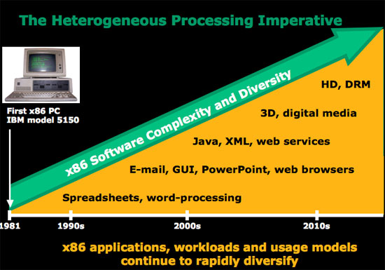
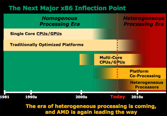
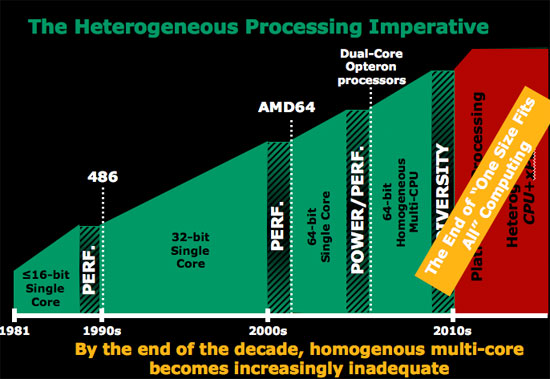
AMD went as far as to say that the next stage in the development of x86 is the heterogeneous processing era. AMD's Phil Hester stated plainly that by the end of the decade, homogeneous multi-core becomes increasingly inadequate. The groundwork for the heterogeneous processing era (multiple cores on chip each with a different purpose) will be laid in the next 2 - 4 years, with true heterogeneous computing coming after 2010.
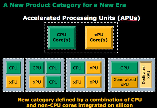
It's not just about combining the CPU and GPU as we know them; it's also about adding other types of processors and specialized hardware. You may remember that Intel made some similar statements a few IDFs ago, but not nearly as boldly as AMD given that Intel doesn't have nearly as strong of a graphics core to begin integrating. The xPUs listed in the diagram above could easily be things like H.264 encode/decode engines, network accelerators, virus scan accelerators, or any other type of accelerator that's deemed necessary for the target market.
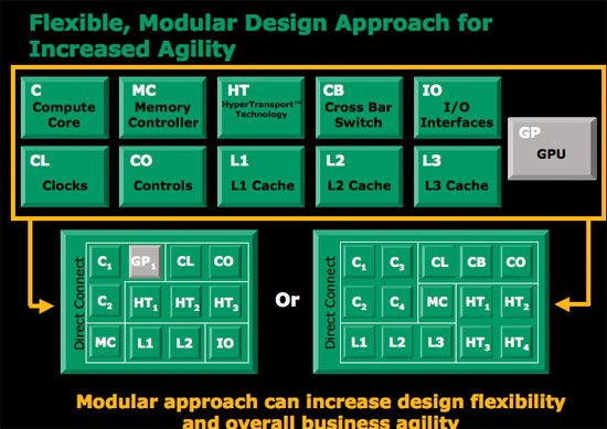
In a sense, AMD's approach is much like that of the Cell processor, the difference being that with AMD's direction the end result would be a much more powerful sequential core combined with a true graphics core. Cell was very much ahead of its time, and by the time AMD and Intel can bring similar solutions to the market the entire industry will be far more ready for them than it was for Cell. Not to mention that treating everything as extensions to the x86 ISA makes programming far easier than with Cell.
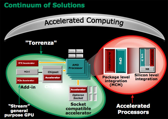
Where does AMD's Torrenza fall into play? If you'll remember, Torrenza is AMD's platform approach to dealing with different types of processors in an AMD system. The idea being that external accelerators could simply pop into an AMD processor socket and communicate with the rest of the system over Hyper Transport. Torrenza actually works quite well with AMD's Fusion strategy, because it allows for other accelerators (xPUs if you will) to be put in AMD systems without having to integrate the functionality on AMD's processor die. If there's enough demand in the market, AMD can eventually integrate the functionality on die, but until then Torrenza offers a low cost in-between solution.
AMD drew the parallel to the 287/387 floating point coprocessor socket that was present on 286/386 motherboards. Only around 2 - 3% of 286 owners bought a 287 FPU, while around 10 - 20% of 386 owners bought a 387 FPU; when the 486 was designed it simply made sense to integrate the functionality of the FPU into all models because the demand from users and developers was there. Torrenza would allow the same sort of migration to occur from external socket to eventual die integration if it makes sense, for any sort of processor.
AMD has already outlined the beginning of its CPU/GPU merger strategy in a little product called Fusion. While quite bullish on Fusion, AMD hasn't done a tremendous job of truly explaining the importance of Fusion. Fusion, if you haven't heard, is AMD's first single chip CPU/GPU solution due out sometime in the 2008 - 2009 timeframe. Widely expected to be two individual die on a single package, the first incarnation of Fusion will simply be a more power efficient version of a platform with integrated graphics. Integrated graphics is nothing to get excited about, but it is what follows as manufacturing technology and processor architectures evolve that is really interesting.

AMD views the Fusion progression as three discrete steps:

Today we have a CPU and a GPU separated by an external bus, with the two being quite independent. The CPU does what it does best, and the GPU helps out wherever it can. Step 1, is what AMD is calling integration, and it is what we can expect in the first Fusion product due out in 2008 - 2009. The CPU and GPU are simply placed next to one another and there's minor leverage of that relationship, mostly from a cost and power efficiency standpoint.
Step 2, which AMD calls optimization, gets a bit more interesting. Parts of the CPU can be shared by the GPU and vice versa. There's not a deep level of integration, but it begins the transition to the most important step - exploitation.
The final step in the evolution of Fusion is where the CPU and GPU are truly integrated, and the GPU is accessed by user mode instructions just like the CPU. You can expect to talk to the GPU via extensions to the x86 ISA, and the GPU will have its own register file (much like FP and integer units each have their own register files). Elements of the architecture will be shared, especially things like the cache hierarchy, which will prove useful when running applications that require both CPU and GPU power.
The GPU could easily be integrated onto a single die as a separate core behind a shared L3 cache. For example, if you look at the current Barcelona architecture you have four homogenous cores behind a shared L3 cache and memory controller; simply swap one of those cores with a GPU core and you've got an idea of what one of these chips could look like. Instructions that can only be processed by the specialized core will be dispatched directly to it, while instructions better suited for other cores will be sent to them. There would have to be a bit of front end logic to manage all of this, but it's easily done.


AMD went as far as to say that the next stage in the development of x86 is the heterogeneous processing era. AMD's Phil Hester stated plainly that by the end of the decade, homogeneous multi-core becomes increasingly inadequate. The groundwork for the heterogeneous processing era (multiple cores on chip each with a different purpose) will be laid in the next 2 - 4 years, with true heterogeneous computing coming after 2010.

It's not just about combining the CPU and GPU as we know them; it's also about adding other types of processors and specialized hardware. You may remember that Intel made some similar statements a few IDFs ago, but not nearly as boldly as AMD given that Intel doesn't have nearly as strong of a graphics core to begin integrating. The xPUs listed in the diagram above could easily be things like H.264 encode/decode engines, network accelerators, virus scan accelerators, or any other type of accelerator that's deemed necessary for the target market.

In a sense, AMD's approach is much like that of the Cell processor, the difference being that with AMD's direction the end result would be a much more powerful sequential core combined with a true graphics core. Cell was very much ahead of its time, and by the time AMD and Intel can bring similar solutions to the market the entire industry will be far more ready for them than it was for Cell. Not to mention that treating everything as extensions to the x86 ISA makes programming far easier than with Cell.

Where does AMD's Torrenza fall into play? If you'll remember, Torrenza is AMD's platform approach to dealing with different types of processors in an AMD system. The idea being that external accelerators could simply pop into an AMD processor socket and communicate with the rest of the system over Hyper Transport. Torrenza actually works quite well with AMD's Fusion strategy, because it allows for other accelerators (xPUs if you will) to be put in AMD systems without having to integrate the functionality on AMD's processor die. If there's enough demand in the market, AMD can eventually integrate the functionality on die, but until then Torrenza offers a low cost in-between solution.
AMD drew the parallel to the 287/387 floating point coprocessor socket that was present on 286/386 motherboards. Only around 2 - 3% of 286 owners bought a 287 FPU, while around 10 - 20% of 386 owners bought a 387 FPU; when the 486 was designed it simply made sense to integrate the functionality of the FPU into all models because the demand from users and developers was there. Torrenza would allow the same sort of migration to occur from external socket to eventual die integration if it makes sense, for any sort of processor.


55 Comments
View All Comments
sprockkets - Friday, May 11, 2007 - link
Yeah, and the cheapest CPU I ever bought was an AMD Sempron for $29.goinginstyle - Friday, May 11, 2007 - link
So with your logic, if the reviews about Barcelona end up being positive and glowing then we know AMD paid off the reviewers?R3MF - Friday, May 11, 2007 - link
I am delighted to hear that AMD is on the bounce, as i have always cheered for them.With the exception of my current C2D PC, i have always bought AMD rigs:
1.2GHz Thunderbird
1.7GHz Thoroughbred
2.0GHz Athlon 64
2.0GHz Athlon X2
So no-one will be more than happy than I to be able to return to the fold, with a shiny new AMD quad-core.
However, if you expect me to buy AMD powered chipsets and graphics cards, then AMD had better pull their socks up on linux support.
I buy nvidia chipsets and graphics cards not because they make better hardware than AMD/ATI, but because i know that i have excellent support in the form of BOTH windows and linux driver support.
Sort that out and I may become an entirely AMD devotee.
If AMD sticks with cack linux drivers along with scuppering nVidia support, then I will wave goodbye to AMD and buy a second Intel/nVidia rig in Autumn this year.
Best of luck AMD, I want you to succeed.
MrJim - Friday, May 11, 2007 - link
Excellent article Anand! Feels very "honest", i think many big corporations must change the way the think about transparency towards the public. Great work.Viditor - Friday, May 11, 2007 - link
Nice article Anand...One point, you stated "By the middle of this year AMD's Fab 36 will be completely transitioned over to 65nm"...
Not to pick nits, but didn't AMD just recently announce that all wafer starts were now 65nm at Fab 36? (or are you speaking of wafer outs...?)