Original Link: https://www.anandtech.com/show/11550/the-intel-skylakex-review-core-i9-7900x-i7-7820x-and-i7-7800x-tested
The Intel Skylake-X Review: Core i9 7900X, i7 7820X and i7 7800X Tested
by Ian Cutress on June 19, 2017 9:01 AM EST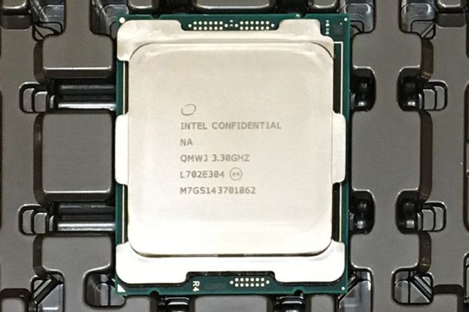
Building a PC is an experience worth having. Finding out what works with what and putting it all together is an experience, and the first time always gives a sense of achievement and accomplishment. In the high-end desktop space, even more so: trying not to break your first $500+ CPU can be akin to feeling like a surgeon. Following the HEDT space can be a journey, especially after five years of iterative updates we are seeing something special happening in 2017. Intel, the incumbent, is changing its 2017 strategy in a few ways which means there is more to understand, and in the future, and also means it is set to release 18-core consumer processors. Today is the first part of that release, with the new Skylake-X processors: the Core i9-7900X, the Core i7-7820X and the Core i7-7800X. These throw a few curveballs into the mix which are worth walking into.
Back at Computex, Intel announced its new high-end desktop (HEDT) platform code named Basin Falls. There are three elements to Basin Falls: the new X299, chipset which brings a number of enhancements from the more mainstream consumer line, a set of Skylake-X processors based on the Skylake-SP microarchitecture (and slightly different from the mainstream Skylake-S processors launched in 2015) from 6 cores to 18 cores, and a pair of Kaby Lake-X processors, reusing the Kaby Lake-S silicon launched earlier this year but with a bit more frequency and power consumption.
We covered all three parts in our launch pieces (linked below), but here is a quick recap.
Intel Announces Basin Falls: The New High-End Desktop Platform and X299 Chipset
Intel Announces Skylake-X: Bringing 18-Core HCC Silicon to Consumers for $1999
Intel Announces Kaby Lake-X Processors: High-End Desktop Getting the Latest Microarchitecture
Skylake-X Today: Three CPUs, Up to 10 Cores, Lower Pricing than Broadwell-E
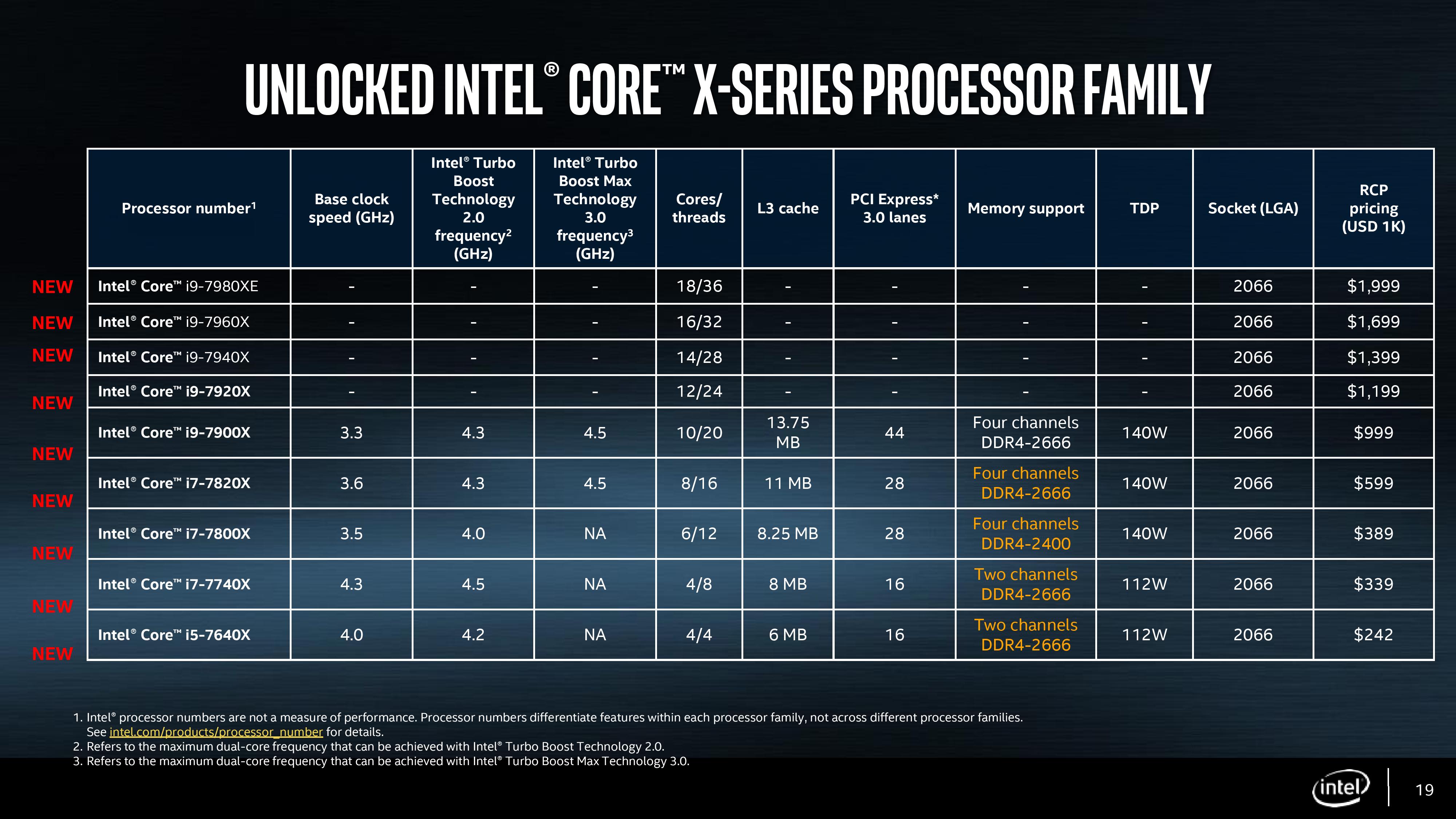
One of the big criticisms from the launch of Broadwell-E, the platform before Skylake-X, was that Intel significantly increased prices over the preceding generation. Nominally consumers were used to the fact that the top chip in the stack was $999 to $1099, and rather than readjust the 6, 8 and 10 core parts to do so, Broadwell-E pushed the 10-core Core i7-6950X to ~$1721, in order to claim parity with the enterprise processors. Users who scoffed at that price will be pleased to hear that the Skylake-X processors launching today are priced more in line with Intel's traditional HEDT chips.
| Skylake-X Processors (Low Core Count Chips) | |||
| Core i7-7800X | Core i7-7820X | Core i9-7900X | |
| Cores / Threads | 6/12 | 8/16 | 10/20 |
| Base Clock | 3.5 GHz | 3.6 GHz | 3.3 GHz |
| Turbo Clock | 4.0 GHz | 4.3 GHz | 4.3 GHz |
| TurboMax Clock | N/A | 4.5 GHz | 4.5 GHz |
| L3 | 8.25 MB | 11 MB | 13.75 MB |
| PCIe Lanes | 28 | 44 | |
| Memory Channels | 4 | ||
| Memory Freq | DDR4-2400 | DDR4-2666 | |
| TDP | 140W | ||
| Price | $389 | $599 | $999 |
The Core i9-7900X is the 10-core processor and set to have a tray price of $999, which means the shelf price will be around $1049-$1099. The Core i9-7900X is also the only one with a full complement of 44 PCIe lanes from the processor, as Intel is restricting this feature to the higher cost parts of the stack in order to further differentiate it from the cheaper i7-7800 series. This processor is quite aggressive in its specifications – normally the top LCC processor is clocked down, using the extra cores as the main reason for purchase, but here Intel is supporting a maximum turbo frequency of 4.3 GHz, or up to 4.5 GHz with the new-ish favored core mode. The base frequency is lower than the other CPUs to compensate, at 3.3 GHz, but we saw an all-core frequency at 4.0 GHz in our testing. This all comes in a 140W TDP, with support up to DDR4-2666 in quad channel mode at 1 DIMM per channel (DDR4-2400 at 2DPC).
The Core i7-7820X sits below, exchanging two of the CPU cores and some PCIe lanes for a higher base frequency. This is an eight-core part, which reduces the total cache as well, but has a base frequency of 3.6 GHz to compensate. The PCIe lanes are reduced from 44 to 28 as part of Intel’s product segmentation strategy, although Intel notes this is still enough for a single GPU and three PCIe 3.0 x4 devices (such as storage) directly attached to the processor. DRAM support is the same as the Core i9 at DDR4-2666, as is also the TDP at 140W. Coming in at $599 represents a bit of a step from the 10-core down to the 8-core. This price will arguably draw a good number of users who would rather direct that $400 to something else in their system with the only deficit being two cores and a proper x16/x16 layout for dual video cards.
The bottom processor is the Core i7-7800X, with six cores, a lower frequency (3.5 GHz base, 4.0 GHz turbo, no favored core support), 28 PCIe lanes, and support only up to DDR4-2400. While categorically ‘the runt’ of the litter, Intel has priced this part at $389, only $50 more than the mainstream consumer quad-core overclocking processors. Along with a slight cost increase for the new X299 motherboards, users looking to move from the mainstream to the bottom rung of the high-end desktop can do so with around $120-$150 extra for CPU+motherboard, and then a bit more if the users wants to use quad channel memory (these processors work in dual channel as well). As the low-end part, traditionally users may point to it as a potential overclocking processor – we unfortunately did not have time to test our sample for overclocking, but I wouldn’t be surprised to see it hit the same frequencies as the other two processors fairly easily.
Competition and Market
In previous years, Intel only had one serious angle of competition for the HEDT platform: itself. As it introduced new generation parts, the older generation could (sometimes) be picked up cheaper, making the older generation more enticing. But as it stands, for the first time in a long time, Intel has three main sources of competition for the X299 platform.
First is as mentioned, Intel’s older platform in Broadwell-E (or even Haswell-E). Broadwell-E, aside from the steep pricing, is now a solid platform, with extensive motherboard support and well-known functionality. Intel has not officially dropped the prices of the older processors, which unless the retailers decide to shift stock wholesale might discourage users going for brand new CPUs, but the ecosystem for BDW-E is mature.
| Comparison: Core i9-7900X vs. i7-6950X vs i7-5960X |
|||
| Features | Intel Core i9-7900X | Intel Core i7-6950X | Intel Core i7-5960X |
| Core | Skylake-SP | Broadwell | Haswell |
| Cores/Threads | 10 / 20 | 10 / 20 | 8 / 16 |
| Base/Turbo | 3.3 / 4.3 GHz | 3.0 / 3.5 GHz | 3.0 / 3.6 GHz |
| PCIe 3.0 Lanes | 44 | 40 | 40 |
| L2 Cache/core | 1 MB | 256 KB | 256 KB |
| L3 Cache | 13.75 MB | 25 MB | 20 MB |
| TDP | 140 W | 140 W | 140 W |
| Price (MSRP) | $999 | $1723 | $999 |
Second is AMD’s recently released Ryzen set of CPUs. As the first new serious entry into the HEDT space for AMD in almost five years, along with a new x86 core, AMD offered similar-ish performance to Broadwell-E in many aspects (within a few percent), but at half the price or better. The Ryzen CPUs still had other limits – dual channel memory, only sixteen PCIe lanes, limited IO from the chipset, and a miasma surrounding the launch with motherboards and memory support; but several months on the ecosystem for Ryzen is fairly solid and still a new and exciting prospect for the HEDT crowd. For $60 less than the price of the Core i7-7800X, a six-core Intel processor, AMD offers the Ryzen 7 1700, which runs in at 8 cores at slightly lower frequency, with cheaper motherboards as well.
| Comparison: Core i7-7800X vs. Ryzen 7 1700 | ||
| Intel Core i7-7800X |
Features | AMD Ryzen 7 1700 |
| 6 / 12 | Cores/Threads | 8 / 16 |
| 3.5 / 4.0 GHz | Base/Turbo | 3.0 / 3.7 GHz |
| 28 | PCIe 3.0 Lanes | 16 |
| 8.25 MB | L3 Cache | 16 MB |
| 140 W | TDP | 65 W |
| $389 | Price (MSRP) | $299 |
Both Intel and AMD would argue the merits of the platforms vs. cost, but Intel still this as an angle for competition. Similarly, the 6-core Core i7-7820X at $599 goes up against the 8-core $499 Ryzen 7 1800X.
| Comparison: Core i7-7820X vs. Ryzen 7 1800X | ||
| Intel Core i7-7820X |
Features | AMD Ryzen 7 1800X |
| 8 / 16 | Cores/Threads | 8 / 16 |
| 3.6 / 4.3GHz (4.5 GHz TMax) |
Base/Turbo | 3.6 / 4.0 GHz |
| 28 | PCIe 3.0 Lanes | 16 |
| 11 MB | L3 Cache | 16 MB |
| 140 W | TDP | 95 W |
| $599 | Price (MSRP) | $439 |
Third is AMD’s future HEDT (or Super High-End Desktop, SHED) platform. Announced in the run up to Computex, AMD is set to offer a new X399 chipset with ThreadRipper processors up to 16-core and with 60 PCIe lanes for graphics (plus four for the chipset, which is why AMD keeps saying 64). AMD is using two of its consumer Zeppelin silicon dies on the same package to get up to 16-cores, and has a new socket planned due to the increase in PCIe support. Having had Intel moving from 6 to 8 to 10 cores on the HEDT space over the last 5-6 years meant that AMD announcing a 16-core part was a big enough jolt to this market such that Intel has to provide a response. Pitting a 10-core CPU such as the Core i9-7900X against a 16-core AMD CPU means that AMD would win most the high-throughput heavily-threaded benchmarks, despite perhaps being lower frequency and higher power. For the HEDT/SHED crowd, sometimes it’s all about how quick you can compute. AMD is set to launch the X399 platform and ThreadRipper CPUs in the summer, so we’re still light on details until then, but given AMD's disruptive nature, there's a real risk to Intel that AMD will once again undercut Intel’s equivalent 16-core pricing by a large amount.
| Comparison: Core i9-7900X vs. i7-6950X vs i7-5960X |
|||
| Features | AMD Ryzen 7 1800X | Intel Core i9-7900X | AMD ThreadRipper |
| Core | Zen | Skylake-SP | Zen |
| Cores/Threads | 8 / 16 | 10 / 20 | 16 / 32 |
| Base/Turbo | 3.6 / 4.0 GHz | 3.3 / 4.3 GHz | ? |
| PCIe 3.0 Lanes | 16 | 44 | 60 |
| L2 Cache/core | 512 KB | 1 MB | 512 KB |
| L3 Cache | 16 MB | 13.75 MB | 32 MB |
| TDP | 95W | 140 W | >140W ? |
| Price (MSRP) | $439 | $999 | ?!? |
What Is This Review
This review comes in two big meaty chunks to sink your teeth into. The first part is discussing the new Skylake-X processors, from silicon to design and covering some of the microarchitecture features, such as AVX-512-F support and cache structure. As mentioned, Skylake-X has some significantly different functionality to the Skylake-S core, which has an impact on how software should be written to take advantage of the new features.
The second part is our testing and results. We were lucky enough to source all three Skylake-X processors for this review, and have been running some regression testing of the older processors on our new 2017 testing suite. There have been some hiccups along the way though, and we’ll point them out as we go.
An extra morsel to run after is our IPC testing. We spend some time to run tests on Skylake-S and Skylake-X to see which benchmarks benefit from the new microarchitecture design, and if it really does mean anything to consumers at this stage.
It should be noted that Intel did not provide all the CPUs for this review. As with standard Intel policy, only the top CPU came direct from Intel. All CPUs in this review are classified as engineering samples for partner testing and not for resale, although they are identical to retail CPUs in performance.
The Basin Falls Platform: X299, SKL-X, & KBL-X
For most practical definitions of the Basin Falls platform, the X299 chipset is the heart. X299 supports the new processors, and like the Z170 and Z270 counterparts on the mainstream consumer line, is basically a big PCIe switch. One of the issues with the older X99 chipset was its limited capabilities, and inability to drive many PCIe devices – this changes with the big switch mentality on X299. For the DMI 3.0 link going into the chipset (basically a PCIe 3.0 x4), the chipset has access to up to 24 PCIe 3.0 lanes for network controllers, RAID controllers, USB 3.1 controllers, Thunderbolt controllers, SATA controllers, 10GbE controllers, audio cards, more PCIe slot support, special controllers, accelerators, and anything else that requires PCIe lanes in either an x4, x2 or x1 link. The total uplink is limited by the DMI 3.0 link, but there will be very few situations where this is saturated. There are a few limits to what support is available (some ports are restricted in what they can handle), and only three PCIe 3.0 x4 drives can use the in-built PCIe RAID, but this should satiate all but the most hardcore enthusiasts.
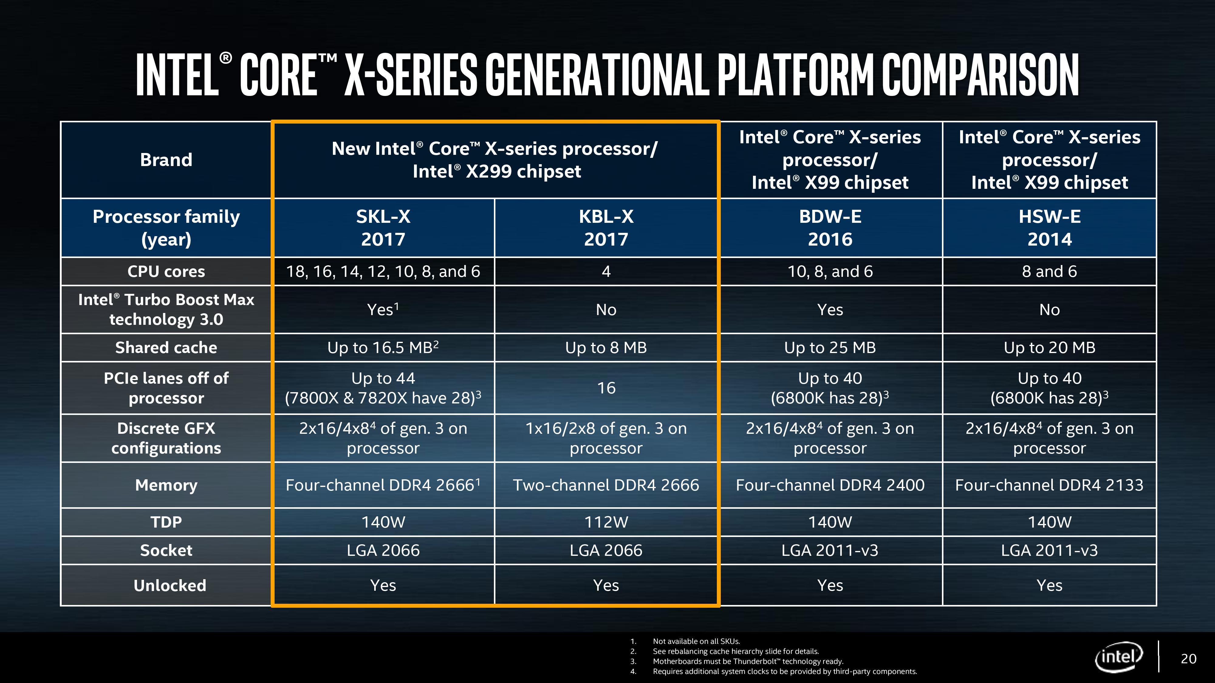
The Skylake-X family of processors for Basin Falls comes in two stages, based on the way the processors are developed. Normally HEDT processors are cut down versions of enterprise processors, usually through restricting certain functions, but the enterprise processors are typically derived from three different silicon layouts during manufacturing. Internally Intel call these three layouts the LCC (low core-count), HCC (high core-count) and XCC (extreme core-count), based on the maximum number of cores they support. Nominally Intel does not disclose which silicon layout they use for which processors, though it is usually straight forward to work them out as long as Intel has disclosed what the configurations of the LCC/HCC/XCC dies are. In this case, Intel has officially left everyone guessing, but the point here is that historically Intel only uses the LCC silicon from the enterprise line for its consumer desktop processors.
In previous generations, this meant either a 6, 8 or 10 core processor at the top of the stack for consumers, with lower core count models being provided by binning/salvaging imperfect CPUs. Each year we expected one of two things: the top-end SKU either gets more frequency, less power, or more cores, and as such the march of progress has been predictable. If you had asked us two months ago, we would have fully expected Skylake-X to top out with LCC silicon at 10 or 12 cores, depending on how Intel was planning the manufacturing part.
So the first element of Intel’s launch is the LCC processors, running up to 10 cores. We previously published that the LCC silicon was 12 cores, but we can now show it is 10 – more on that later. The three Skylake-X CPUs launching today are using LCC silicon with 6, 8 or 10 cores as the Core i7-7800X, Core i7-7820X and Core i9-7900X respectively. Intel is further separating these parts by adjusting the level of official supported DRAM frequency, as well as the PCIe lanes. We’ll go in a bit more detail further in the review.
The second element to the Skylake-X launch is the one that has somewhat surprised most of the industry: the launch will contain four processors based on the HCC silicon. Technically these processors will not be out until Q4 this year (one SKU coming out in August), and the fact that Intel did not have frequency numbers to share when announcing these parts shows that they are not finalized, calling into question when they were added to the roadmap (and if they were a direct response to AMD announcing a 16-core part for this summer). We’ve written a detailed analysis on this in our launch coverage, and we’ll cover some of the topics in this review. But Intel is set to launch 12, 14, 16 and 18-core consumer level processors later this year, with the top part running a tray price (when you buy 1k CPUs at a time) of $1999, so we expect the retail to be nearer $2099.
It should be noted that due to a number of factors, the Skylake-X cores and the communication pathways therein are built slightly differently to the consumer version of Skylake-S, which is something discussed and analyzed in this review.
The final element to the Basin Falls launch is Kaby Lake-X. This is also an aspect of the Basin Falls platform that deviates from the previous generations. Intel’s HEDT line has historically been one generation behind the mainstream consumer platform due to enterprise life cycles as well as the added difficulty of producing these larger chips. As a result, the enterprise and HEDT parts have never had the peak processing efficiency (IPC, instructions per clock) of the latest designs and have sat in the wings, waiting. By bringing the Kaby Lake microarchitecture to HEDT, this changes the scene, albeit slightly. Rather than bringing a new big core featuring the latest microarchitecture, Intel is repurposing the Kaby Lake-S mainstream consumer silicon, binning it to slightly more stringent requirements for frequency and power, disabling the integrated graphics, and then putting it in a package for the high-end desktop platform. There are still some significant limitations, such as having only 16 PCIe 3.0 lanes and dual channel memory, which might exclude it from the traditional designation of being a true HEDT processor, however Intel has stated that these parts fill a request from customers to have the latest microarchitecture on the HEDT platform. They also overclock quite well, which is worth noting.
The Kaby Lake-X parts will consist of a Core i7 and Core i5, both of which are quad core parts, with the i7 supporting hyperthreading. We have a parallel Kaby Lake-X review alongside our Skylake-X coverage, with some numbers from a stable 5 GHz overclock.
Microarchitecture Analysis
When Intel announced Skylake-S, the Intel Developer Forum soon followed which shed some light on the underlying microarchitecture. While conceptually using the same paradigm since Sandy Bridge, the Core microarchitecture plan has adapted and changed based on tools and capabilities: more buffers, lower latency, libraries optimized for power, throughput, latency and frequency, and support for new instructions plus better ways to do them. One of those marches has been towards better SIMD performance: clustering multiple data entries into a single element and performing the same operation to each of them at once in one go. This has evolved in many forms, from SSE and SSE2 through AVX and AVX2 and now into AVX-512 (technically AVX-512-F + some others). The goal here is that with the right memory subsystem in place, as long as you can keep the units fed with data and instructions, peak throughput for the data can rise substantially compared to a standard INT or FP execution port.
The new core for Skylake-X, technically called the Skylake-SP core from the Intel Xeon Scalable Platform on the enterprise side, beefs up the cores from the previous Broadwell-E HEDT platform all around while also adjusting the cache hierarchy and adding features. As Intel has yet to create separate entries for the new core (we are being told to wait for the enterprise launch for this information), the following info is Skylake-S based with additional information on the new Skylake-SP core.
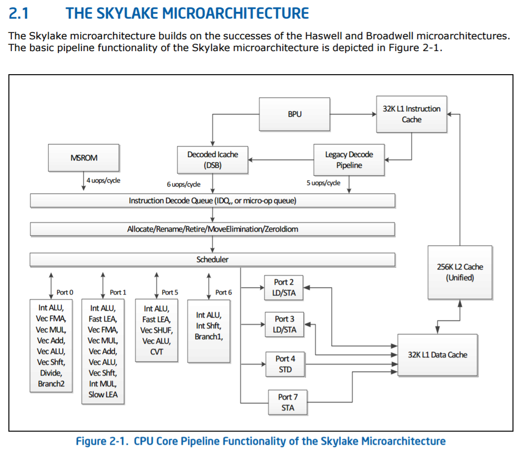
Skylake-S High-Level Core Diagram, from Intel’s Architecture Manual
The base Skylake-S back-end is a six-wide decode using five decoders (four simple, one complex) combined with a 1536 instruction micro-op cache (sometimes called a decoded i-cache) that can support five micro-ops per cycle for instructions that have previously been decoded recently. Instructions that are longer than four micro-ops are served from the MSROM, which can manage 4 micro-ops per cycle. Intel states that the decoders are fed through a more advanced branch prediction unit for Skylake-S over Broadwell-E
These feed into the main instruction queue and out-of-order window, which for Skylake-S was increased to 224 instructions compared to 192 in Haswell. The loop detector in the instruction decode queue can detect loops up to 64 micro-ops per processor, irrespective of hyperthreading. The allocation queue, which also implements rename/retire and other features, follows with 64 entries per thread and is a statically partitioned element of the design (without HT, it will support 128). This feeds into the scheduler, where historically Intel uses a combined scheduler for INT and FP entries. Technically this scheduler can be filled with 180 INT and 168 FP entries, up from 168/168 in Haswell, which can dispatch one micro-op per cycle to each of the eight ports.
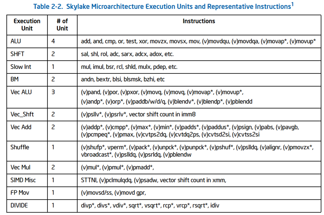
The ports are split as in the diagram, with two load/store units, one dedicated store address unit and one dedicated store data unit. The four ALU ports support a subset of all the ALU features, which Intel states has been balanced over Haswell. The full breakdown is as follows:
- Port 0: ALU/Vec ALU, Vec Shft/Vec Add, Vec Mul/FMA, DIV, Branch2
- Port 1: ALU/Vec ALU/Fast LEA, Vec Shift/Vec Add, Vec Mul/FMA, Slow Int, Slow LEA
- Port 2: Load/Store Address
- Port 3: Load/Store Address
- Port 4: Store Data
- Port 5: ALU/Vec ALU/Fast LEA, Vec Shuffle, (FMA on 10-core SKL-X)
- Port 6: ALU/Shift, Branch1
- Port 7: Store Address
Due to this arrangement, there are only certain combinations of instructions that can be run concurrently – e.g. you can’t put a vector operation across each and every port at once. Intel gives the following guidelines:
Nominally the FMAs on ports 0 and 1 are 256-bit, so in order to drive towards the AVX-512-F these two ports are fused together, similar to how AVX-512-F is implemented in Knights Landing. The six-core and eight-core Skylake-X parts support one fused FMA for AVX-512-F, although the 10-core will support dual 512-bit AVX-512-F ports, which seems to be located on port 5. This means that the 10-core i9-7900X can support 64 SP or 32 DP calculations per cycle, whereas the 8-core/6-core parts can support 32 SP or 16 DP per cycle.
Through the system, up to 72 loads in-flight and 56 stores in-flight are supported, up from 72/42 in Haswell. Some of the instructions have also changed in latency, such as moving to a Radix-1024 divider which brings the division latency from 3-cycles to 5-cycles (we were told that this just helps arrange everything for energy, power and layout). Other instructions typically follow the Skylake-S guidelines, although Intel is holding some information back for the official Skylake-SP launch.
The four load/store related units serve the writeback 32KB L1 Data cache with 8-way associativity and 4-cycle latency. In Skylake-S, this supported two 32-byte reads and one 32-byte store per cycle: in the new Skylake-SP core, this is doubled although Intel only stated that it was ‘128 bytes per cycle read and 64 bytes per cycle write’, which we would assume to mean 2x64B read and 1x64B write. This is backed by an L1D TLB, supporting 64x4KB entries per thread with 4-way associativity.
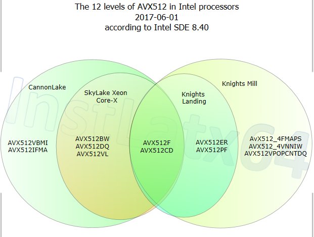
AVX-512? AVX-512-F?
Intel is introducing several variations of the new AVX-512 instruction support, based on the hardware and market segmentation. Ultimately there is one underlying set of AVX-512 instructions supported, and the different variants add different instructions.
AVX-512-F: F for Foundation
AVX-512-BW: Support for 512-bit Word support
AVX-512-CD: Conflict Detect (loop vectorization with possible conflicts)
AVX-512-DQ: More instructions for double/quad math operations
AVX-512-ER: Exponential and Reciprocal
AVX-512-IFMA: Integer Fused Multiply Add with 52-bit precision
AVX-512-PF: Prefetch Instructions
AVX-512-VBMI: Vector Byte Manipulation Instructions
AVX-512-VL: Foundation plus <512-bit vector length support
AVX-512-4VNNIW: Vector Neural Network Instructions Word (variable precision)
AVX-512-4FMAPS: Fused Multiply Accumulation Packed Single precision
We expect there to be FPGA related AVX-512 support in this mix as well at some point.
Nominally these different AVX-512 features are meant to be supported directly by the hardware and enabled therein. It might be possible that the standard AVX-512 block that Intel uses will have features enabled/disabled at a firmware level and users/software may have to be activated/approved to use certain features. Because AVX-512 is designed more for enterprise workloads, these focused instruction sets are unlikely to be part of the consumer workload, but it is worth noting that when someone says ‘AVX-512 support’, you should ask which level of AVX-512 they mean.
We’ve already seen a form of AVX-512 in the latest Xeon Phi processors, Knights Landing (KNL), which support AVX-512-F, AVX-512-CD, AVX-512-ER and AVX-512-PF. The latest KNL chips use 72 Atom Silvermont-class cores arranged as 36 pairs, combined with two AVX-512-units per pair, 16GB of MCDRAM and as much memory bandwidth as you can shake a stick at. The base cores in Knights Landing are slow – 1.2 GHz, but combine that with a potential 32 DP operations per AVX unit, and it’s an impressive machine.
Intel has hinted at future AVX-512 instructions in software development environments, allowing programmers to target certain instructions and get their software ready.
From @InstLatx64
As with previous versions of AVX, when these instructions are needed the CPU will have to reduce frequency in order to maintain stability. In silicon these pathways are densely packed and draw a lot of power, so with AVX instructions, and even more so with AVX-512-F, in order to balance power, voltage drop and the resulting temperature rise, AVX-512-F will run at a lower frequency than AVX/AVX2, and a lower frequency than other core instructions.
Given what we know about the AVX-512 units in Knights Landing, we also know they are LARGE. Intel quoted to us that the AVX-512 register file could probably fit a whole Atom core inside, and from the chip diagrams we have seen, this equates to around 12-15% of a Skylake core minus the L2 cache (or 9-11% with the L2). As seen with Knights Landing, the AVX-512 silicon takes up most of the space.
So with Skylake-X, the cores support F, VL, BW, DQ and CD. This gives a range of potential applications with code moving forward.
What Can Be Done With AVX-512 in a Skylake-SP core?
Intel went into detail about what the AVX-512 units can do and how it is supported.
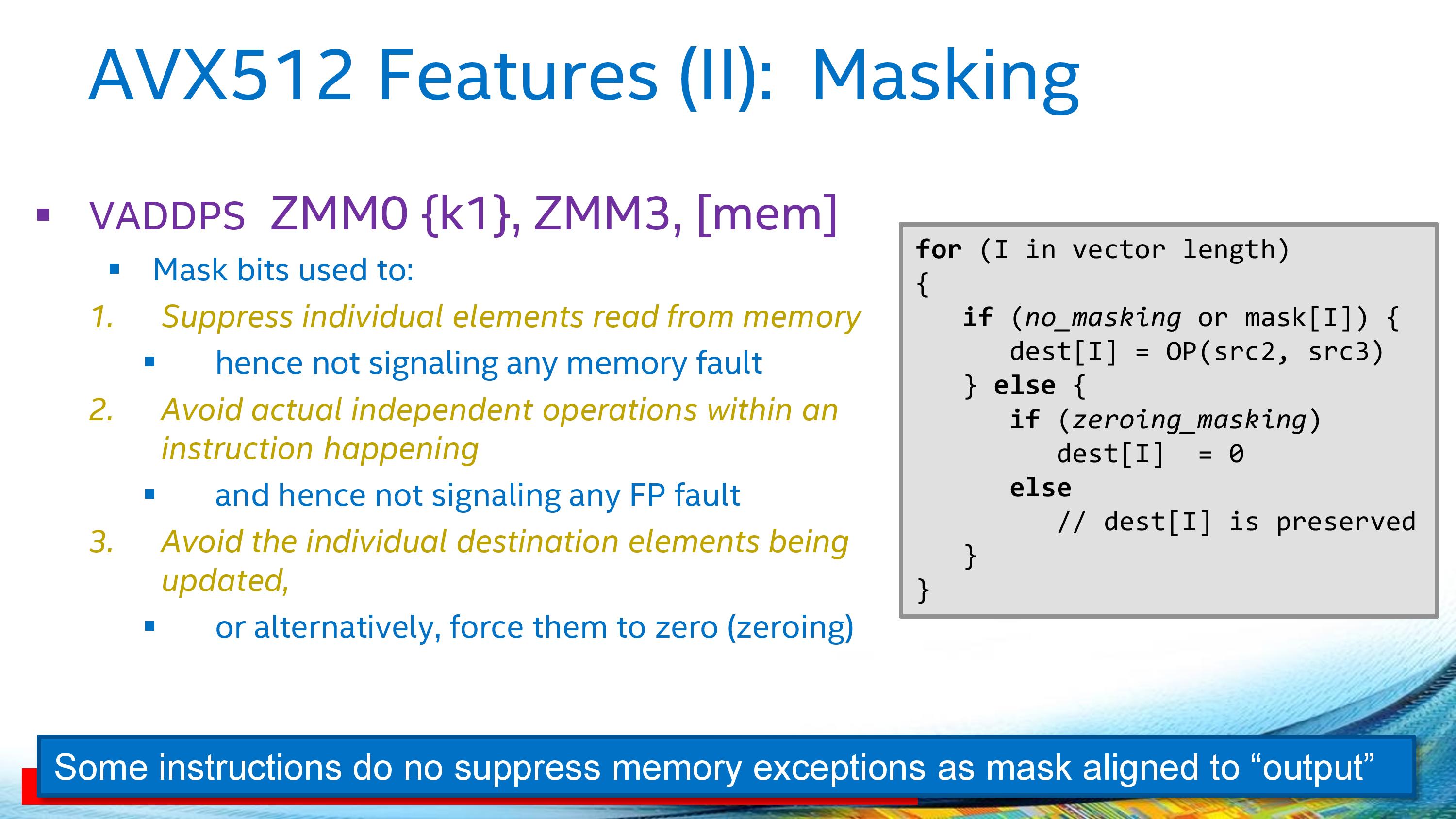
The Skylake-SP core supports separate Mask Registers, which allows Boolean decision operations to be separated into their own silicon rather than take up vector register space (there’s no point storing one bit in a 64-bit register…). This should allow programmers to separate control flow from data flow, especially for such features as encoding as well as reducing energy for logical predicates (performing a check on a mask register consumes less power than a regular register). The AVX-512-F unit supports 512-bit INT/FP calculations from 32 zmm (zmm0 to zmm31) registers, supported by 8 kmask (k0 to k7).

The mask registers can also be used to implement a technique called masking, ensuring individual elements in the main registers can be updated and bypassing potential memory faults, as some instructions (such as VADDPS) do not express memory exceptions and this technique allows the programmer to bypass the known exception event with new data or direct to zero.
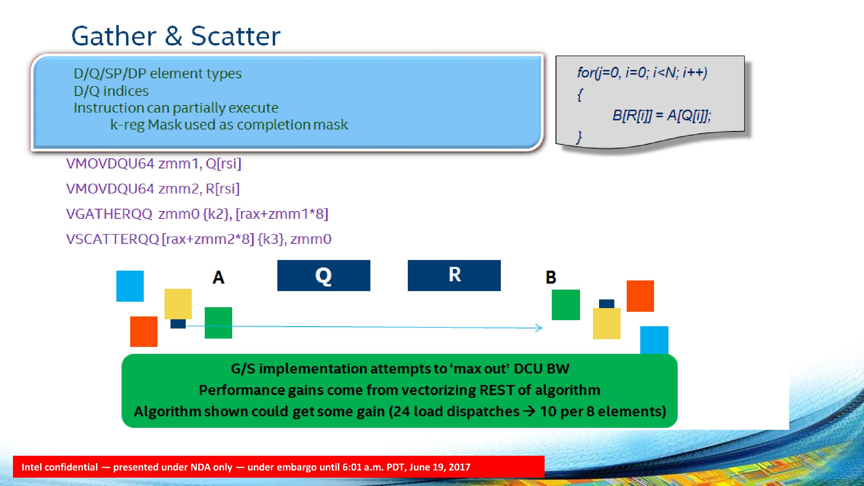
The Skylake-SP core through the AVX-512 also gives native support for 64-bit integers, which allows for basic control functionality to be vectorized and natively supported. Intel cites shift operations and logical operations as the obvious examples, but it also allows vectorization of long integer math as well as pointer codes. Apparently some program software still had edge cases where this function would have to go to x87 in older microarchitectures. The 64-bit support is also important when it comes to gather and scatter operations. Combining this with the masking support allows bandwidth to be maximized in gather/scatter operations and put the emphasis back on other functions in the code.
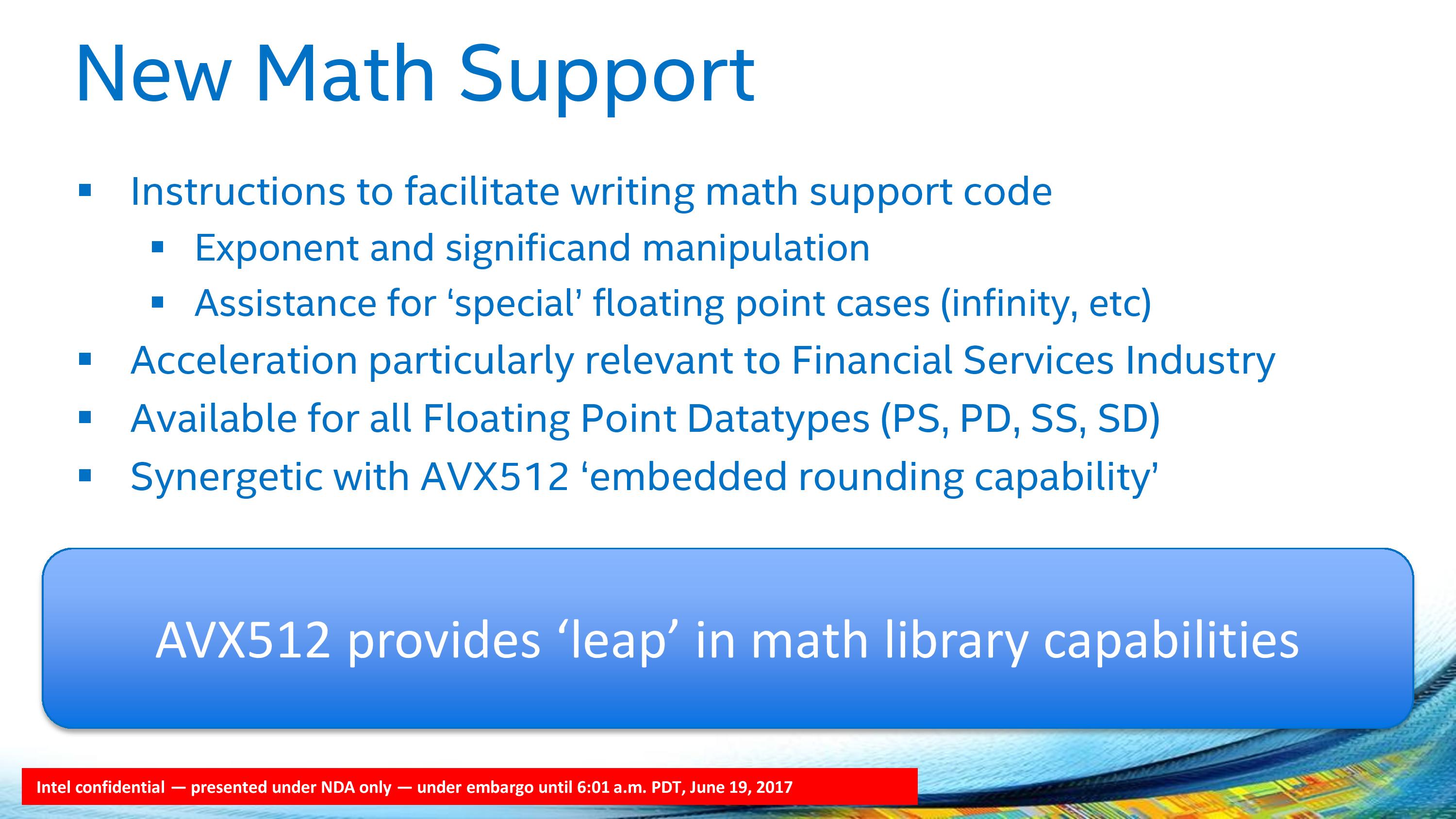
The AVX-512 unit will also allow for additional math support. Scalar, SSE and AVX code can be promoted, but also rounding is embedded with instructions for exponent and significand modification as well as assistance in potential undefined cases (inf, -inf). These new operations can be supported for all FP datatypes (PS, PD, SS, SD), and we are told that this is most important to the financial services industry. We were told that outside financial services, this feature might be of limited use. The AVX-512-F unit will also support packed computations, such as 8-bit and 16-bit dot product support for deep learning, similar to what we have seen with NVIDIA’s tensor cores (8-bit dot products with 32-bit accumulation: SKL-SP can support >40 8-bit multiply-accumulate operations with 32-bit accumulation per core per cycle).
Bit manipulation and packed rotate functions are also given in the new core, allowing an arbitrary three-entry truth table to be implemented in conjunction with the mask registers. This is going to have a big effect for non-ASIC cryptography when the software catches up.
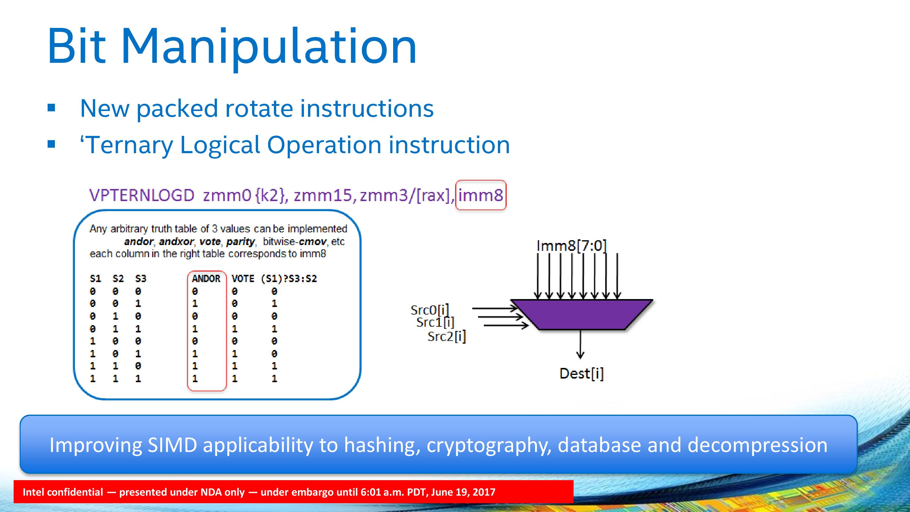
One of the big things that Intel is suggesting about the new AVX-512 unit in the Skylake-SP core is that because of the wide-ranging capabilities, as long as the compilers come on board, it is easier to promote regular code to AVX-512 than it was to SSE/AVX. Fundamentally Intel wants to see the compilers get on board and for the faster throughput of regular software to increase performance. If anyone has recompiled old code under a new compiler and had a performance uplift will know exactly what this might entail (recently POV-Ray recompiled their code for the first time in years, moving from VS2010 to VS2015 – instant 15-25% speed up on the newest microarchitectures).
As mentioned above, the AVX-512 unit is per core, and although more aimed at the enterprise crowd, regular software might take a while to catch up. For anyone on the consumer side who wants to play with AVX-512, it is worth reiterating that there is a separation between the Skylake-X processors: the 6-core and 8-core parts only support one FMA per core, whereas the 10-core supports two FMAs per core.
I Keep My Cache Private
As mentioned in the original Skylake-X announcements, the new Skylake-SP cores have shaken up the cache hierarchy compared to previous generations. What used to be simple inclusive caches have now been adjusted in size, policy, latency, and efficiency, which will have a direct impact on performance. It also means that Skylake-S and Skylake-SP will have different instruction throughput efficiency levels. They could be the difference between chalk and cheese and a result, or the difference between stilton and aged stilton.
Let us start with a direct compare of Skylake-S and Skylake-SP.
| Comparison: Skylake-S and Skylake-SP Caches | ||
| Skylake-S | Features | Skylake-SP |
| 32 KB 8-way 4-cycle 4KB 64-entry 4-way TLB |
L1-D | 32 KB 8-way 4-cycle 4KB 64-entry 4-way TLB |
| 32 KB 8-way 4KB 128-entry 8-way TLB |
L1-I | 32 KB 8-way 4KB 128-entry 8-way TLB |
| 256 KB 4-way 11-cycle 4KB 1536-entry 12-way TLB Inclusive |
L2 | 1 MB 16-way 11-13 cycle 4KB 1536-entry 12-way TLB Inclusive |
| < 2 MB/core Up to 16-way 44-cycle Inclusive |
L3 | 1.375 MB/core 11-way 77-cycle Non-inclusive |
The new core keeps the same L1D and L1I cache structures, both implementing writeback 32KB 8-way caches for each. These caches have a 4-cycle access latency, but differ in their access support: Skylake-S does 2x32-byte loads and 1x32-byte store per cycle, whereas Skylake-SP offers double on both.
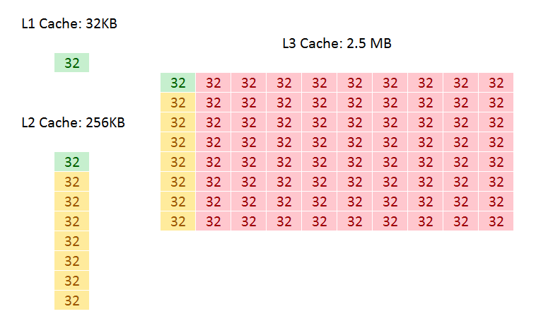
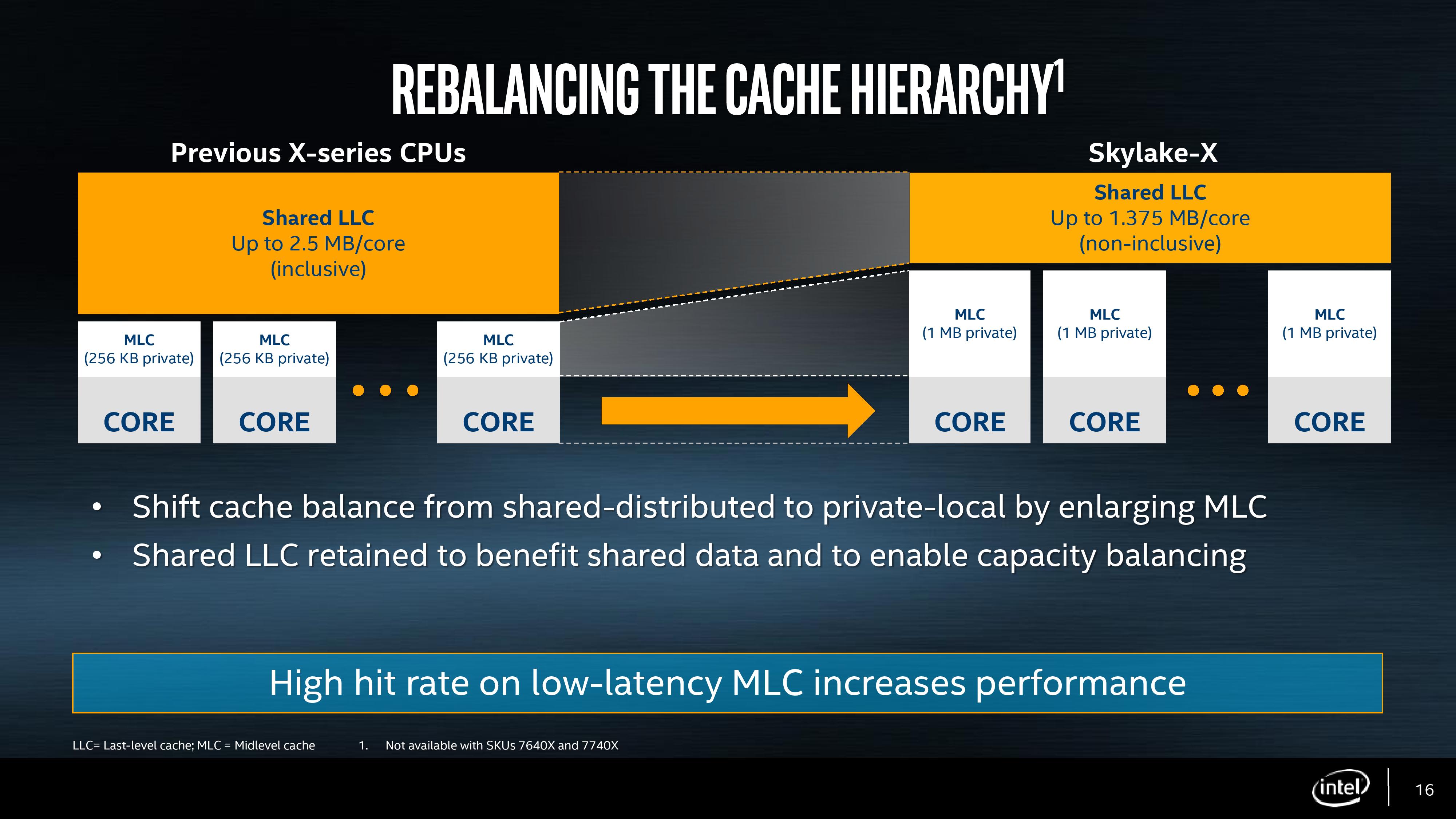
The big changes are with the L2 and the L3. Skylake-SP has a 1MB private L2 cache with 16-way associativity, compared to the 256KB private L2 cache with 4-way associativity in Skylake-S. The L3 changes to an 11-way non-inclusive 1.375MB/core, from a 20-way fully-inclusive 2.5MB/core arrangement.
That’s a lot to unpack, so let’s start with inclusivity:
Inclusive Caching
An inclusive cache contains everything in the cache underneath it and has to be at least the same size as the cache underneath (and usually a lot bigger), compared to an exclusive cache which has none of the data in the cache underneath it. The benefit of an inclusive cache means that if a line in the lower cache is removed due it being old for other data, there should still be a copy in the cache above it which can be called upon. The downside is that the cache above it has to be huge – with Skylake-S we have a 256KB L2 and a 2.5MB/core L3, meaning that the L2 data could be replaced 10 times before a line is evicted from the L3.
A non-inclusive cache is somewhat between the two, and is different to an exclusive cache: in this context, when a data line is present in the L2, it does not immediately go into L3. If the value in L2 is modified or evicted, the data then moves into L3, storing an older copy. (The reason it is not called an exclusive cache is because the data can be re-read from L3 to L2 and still remain in the L3). This is what we usually call a victim cache, depending on if the core can prefetch data into L2 only or L2 and L3 as required. In this case, we believe the SKL-SP core cannot prefetch into L3, making the L3 a victim cache similar to what we see on Zen, or Intel’s first eDRAM parts on Broadwell. Victim caches usually have limited roles, especially when they are similar in size to the cache below it (if a line is evicted from a large L2, what are the chances you’ll need it again so soon), but some workloads that require a large reuse of recent data that spills out of L2 will see some benefit.
So why move to a victim cache on the L3? Intel’s goal here was the larger private L2. By moving from 256KB to 1MB, that’s a double double increase. A general rule of thumb is that a doubling of the cache increases the hit rate by 41% (square root of 2), which can be the equivalent to a 3-5% IPC uplift. By doing a double double (as well as doing the double double on the associativity), Intel is effectively halving the L2 miss rate with the same prefetch rules. Normally this benefits any L2 size sensitive workloads, which some enterprise environments such as databases can be L2 size sensitive (and we fully suspect that a larger L2 came at the request of the cloud providers).
Moving to a larger cache typically increases latency. Intel is stating that the L2 latency has increased, from 11 cycles to ~13, depending on the type of access – the fastest load-to-use is expected to be 13 cycles. Adjusting the latency of the L2 cache is going to have a knock-on effect given that codes that are not L2 size sensitive might still be affected.
So if the L2 is larger and has a higher latency, does that mean the smaller L3 is lower latency? Unfortunately not, given the size of the L2 and a number of other factors – with the L3 being a victim cache, it is typically used less frequency so Intel can give the L3 less stringent requirements to remain stable. In this case the latency has increased from 44 in SKL-X to 77 in SKL-SP. That’s a sizeable difference, but again, given the utility of the victim cache it might make little difference to most software.
Moving the L3 to a non-inclusive cache will also have repercussions for some of Intel’s enterprise features. Back at the Broadwell-EP Xeon launch, one of the features provided was L3 cache partitioning, allowing limited size virtual machines to hog most of the L3 cache if it was running a mission-critical workflow. Because the L3 cache was more important, this was a good feature to add. Intel won’t say how this feature has evolved with the Skylake-SP core at this time, as we will probably have to wait until that launch to find out.
As a side note, it is worth noting here that Broadwell-E was a 256KB private L2 but 8-way, compared to Skylake-S which was a 256KB private L2 but 4-way. Intel stated that the Skylake-S base core went down in associativity for several reasons, but the main one was to make the design more modular. In this case it means the L2 in both size and associativity are 4x from Skylake-S by design, and shows that there may be 512KB 8-way variants in the future.
The New Core-to-Core Communication Paradigm
Within the last week, Intel released a surprising announcement regarding the capability of its upcoming Skylake-SP processors ahead of any official announcement and release, and the relevance of it extends through to the Skylake-X chips as well. With a multi-core design, how cores communicate can be vital, when sharing data between them or by accessing each other’s cache via snooping or having to go out to main memory.
In previous generations, Intel has championed its ring bus strategy. Pretty much every commercial multi-core chip Intel has released uses some form of ring bus, and it boils down to a single communication ring on which all the cores are connected. If data needs to a certain core, it travels on the ring until it reaches the core it needs. The idea is relatively simple, and has worked quite well. It does mean that there is a range of core-to-core latencies however, depending on how far away the core is.
Imagine connecting to a network of computers, but you could only connect to the two computers either side of you. If you needed to speak to a computer that was 5 nodes away, the data would have to travel through each of the nodes to get there. Welcome to the ring bus. The speed of this ring bus was typically denoted by the ‘uncore’ frequency.
With Intel’s three-die program on its enterprise chips, each one used different variants of the ring bus topology. On Broadwell-E, the 10-core LCC design used a single ring bus for all 8 cores and the DRAM controller/PCIe root complex, whereas the HCC and XCC designs both had dual ring buses that used router communication methods to talk between each other. Now obviously talking to a core on the other ring bus added latency, and was sometimes considered a ‘non-uniform memory access’ (NUMA) environment on chip, with extra latency if you needed data from memory on the other ring bus. (Typically NUMA is applied to dual socket platforms, where the DRAM on the other chip has a large delay.) Intel emphasized that the Broadwell-E design was memory location aware, and tried to keep relevant data local to the core it was needed on.
With the larger XCC CPUs for Broadwell-E, the ring buses become quite cumbersome: you end up with one ring bus servicing 12 cores, and another ring bus servicing 12 cores (due to the layout with other elements of the chip).
As more and more cores get added, what is the solution? More ring buses? How about a 2D array of ring buses? Or even a mesh or a network?

The announcement that Intel made in the past week was that Skylake-SP processors will use a mesh topology, whereby each CPU in the design will be connected to the ones above, below, and to the side. Earlier in the week I mentioned on Twitter that a mesh in this context, or as drawn above, is just an array of ring buses in a 2D arrangement, although new information has come to light.
There are several things to talk about the mesh here, so in no particular order:
Mesh Me Up
Intel already sells chips with mesh connectivity: the latest Xeon Phi Knights Landing many-core processors. These massive (~646mm2) chips have 72 cores arranged as 36 pairs, six memory channels and 16GB of MCDRAM, and using a ring bus (or a succession of ring buses) is probably not feasible.
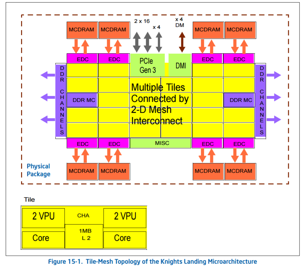
For KNL, Intel calls the mesh the ‘untile’. Taken from the KNL optimization guide:
‘At each mesh stop, there is a connection to the tile and a tag directory that identifies which L2 cache (if any) holds a particular cache line. [In Knights Landing] there is no shared L3 cache within a physical package, [so] memory accesses that miss in the tile must go over the mesh to the tag directory to identify any cached copies in another tile. Cache coherence uses the MESIF protocol. If the cache line is not cached in another tile, then a request goes to memory.’
Knights Landing can run in a variety of mesh modes, due to the lack of an L3 but the presence of an intermediary MCDRAM layer, certain modes to do with the memory hierarchy help with different codes. It is not known if Skylake-SP will have the same feature set.
When distributing cores along a mesh, another way to think about it is as a big routing environment. There are two ways – each core could talk to a central processing router which then sends information as it is needed, or each core acts as a networking point itself, forwarding packets in the direction it is needed. The first method, commonly known as a crossbar method, is easier to implement but can be bottlenecked very easily, not to mention power hungry if the whole crossbar needs to be enabled all the time. The second method, where every core is a router node, looks like what we have already in the image Intel provided.
The announcement Intel made was done officially by Dr Akhilesh Kumar, one of Skylake-SP’s CPU architects. He has been at Intel for a number of years, and digging back through releases with his name on popped up a very interesting paper regarding how to implement a router-like mesh in a multi-core environment, published in March 2014 which is about the right time when Skylake-SPs mesh was being developed. We haven’t had confirmation from Intel that this is how Skylake-SP’s mesh is actually like, though it is worth covering what is in the paper.
For anyone interested, the paper is called MoDe-X: Microarchitecture of a Layout-Aware Modular Decoupled Crossbar for On-Chip Interconnects, IEEE Transactions on Computers, Vol. 63, No. 3, March 2014 P622.
MoDe-X: Is This Skylake-SP’s Mesh?
As mentioned above, the easiest way for a mesh/router is through a crossbar. When the design instead uses each core as a node in the mesh, the result is essentially a ‘mini’ decoupled crossbar in each core acting as the director for data coming in and out of the core. With each core in control of its own actions, the design becomes modular. Put these elements together, and you have a MOdular DEcoupled Crossbar, or MoDe-X.
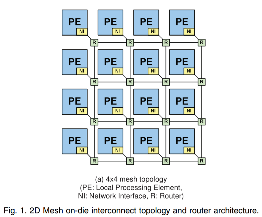
Each core has an integrated network interface and a router, with each router connected to the four routers around it (or 2 routers for corners and 3 routers for edges). A data packet can come in one of five directions – north, south, east, west, or from the core the router is attached to. The data packet then needs to be sent to one of five directions again: north, south, east, west, or to the core the router is attached to. If each core is essentially a node on a 2D map with an x-ordinate and a y-ordinate, if a packet needs to go to (0,0), the router can send it on its way as it knows which nodes are nearest to it. There are algorithms designed to reduce congestion, such as only moving in the x-direction until you are correct then start moving in the y-direction, but a basic system will have buffers and queues and will know how busy the local network congestion is.
The default way to design the router is to take the date from every input, decided where to send it, then send it. The MoDe-X design does it a little differently, and essentially splits the directions up into three groups: one group is north/south, one group is east/west, and the local core is the third group. The following diagram is a bit complex, but we’ll go through it:
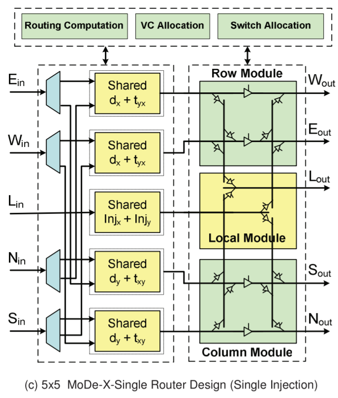
On the left are the five inputs: E, W, L (local), N, S.
On the right are the five outputs, W, E, L, S, N
The first column of ‘shared’ boxes determines where the data wants to go: does it need to traverse a row, a column, or stay local. From each input, there are only two arrows going to either the top pair or the bottom pair of ‘shared’ boxes. Depending on contention and allocation, the data is then sent to the second column whereby if the data needed to change columns, it could either go to Sout or Nout and if it needed to change rows into Wout or Eout. In both circumstances the data could go to the local node.
In the research paper, there is a six-input design which modifies the local input in order to make the wiring in the second half of the design easier (and it lowers power), but the image above is a fair representation of the idea. There are other additions in the paper as well, with layout aware arrangements (how exactly you put it together in silicon) as well as feeder wires such that if data needs to continue in the same direction it can do so with less effort.
The paper is very dense (it took me a while to get to grips with it), but worth a read if you are interested. I found it easier to consider it more like a router, than an on-chip mesh. As mentioned, this is a 2014 paper, and shows simulation data on an 8x8 grid of cores, where this design is both lower power and smaller area than a generic mesh design or competing designs. There were some areas where the generic design had marginally better latency, but the power conservation numbers (due to the wiring reduction and an aggressive power gating scheme to disable certain parts for up to 99% less power use) makes it a more attractive option (especially in multi-core CPUs). Intel was doing simulation work in early 2014 (which means 2013), and the paper mentions that they were in the process of putting these ideas into silicon. It wouldn’t be too far-fetched to consider that this is what we are seeing today.
Die Size Estimates and Arrangements
On the previous page, we showed pictures of ring bus and mesh arrangements. With a ring bus, ultimately the silicon layout of the cores and the interconnects can be regular but are not that stringent. Put the cores in a circle (or overlapping circles) and away you go. With a mesh, things get a little more rigid.
The mesh diagrams on the previous page are all presented as rectangles in x*y arrangements. You either have to add a full row or a full column to increase the die count, whereas in a ring it could be straight forward just to add another pair of cores into the ring (which is what happened over the last few generations). Adding a pair of cores in a mesh means that you end up with more corners and more edges – not all cores end up ‘equal’ and there can be performance penalties therein. Ideally, an arrangement where x = y is usually the best bet. This lets us make some predictions about how Intel’s silicon is lining up.
A side-note for discussion. If we had a 100x100 core arrangement, the cores in the middle would have big latency to get anywhere near external memory. Also, a 2D mesh could become a 3D mesh.
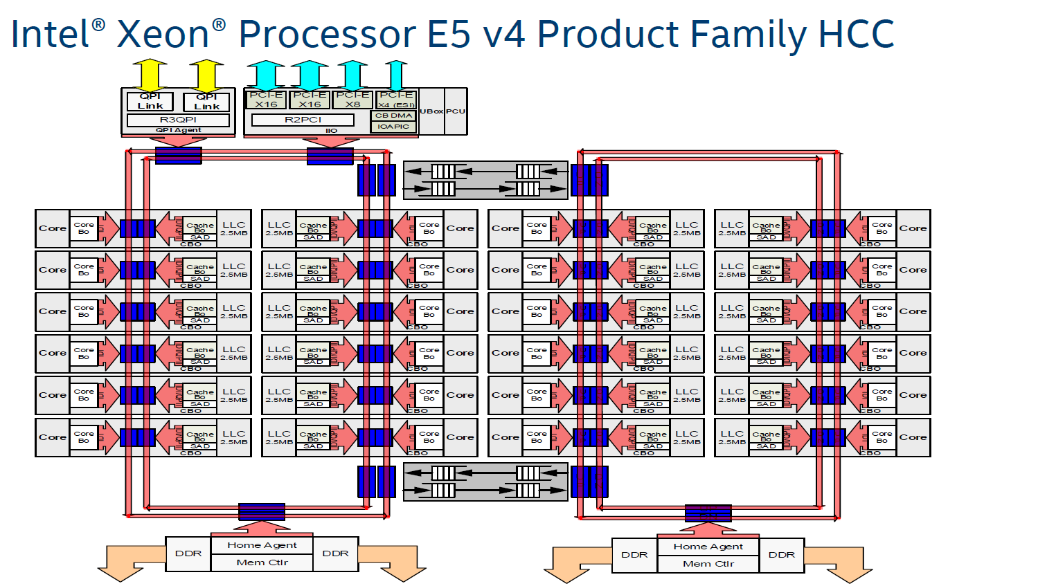
Three things come to our aid in discussing the LCC and HCC silicon. First was the original Skylake-X announcement back at Computex: one of Intel’s slides had an image of the basic floorplan of the HCC silicon to be used for the high core-count Skylake-X processors:
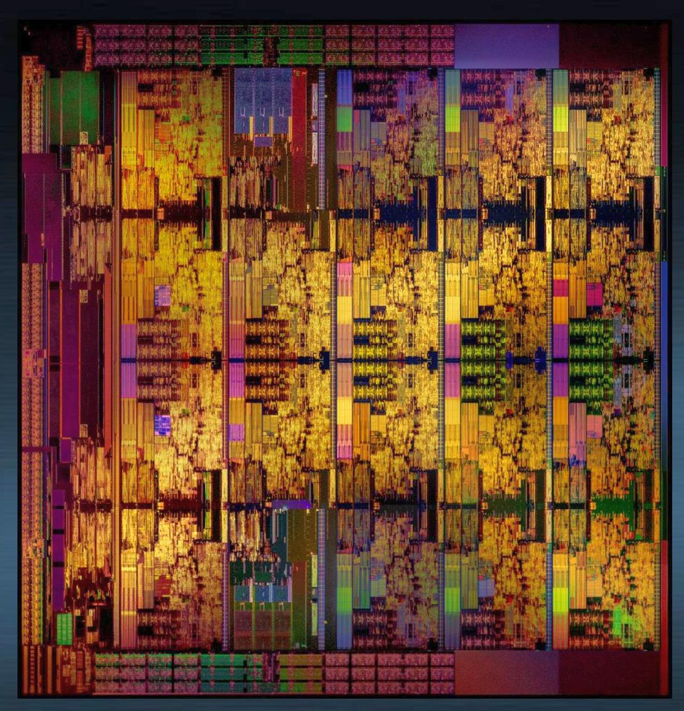
At the time, we were a bit stumped by this image. By counting the regular structures, we can see 4x5 arrangement, or rather a 20-core chip. On closer inspection two of the cores were different: on the second column, the top and bottom ‘cores’ did not look like cores. At the time we postulated that given the size of AVX512, this might be where they were. But the second piece of information was given through Intel’s mesh announcement.
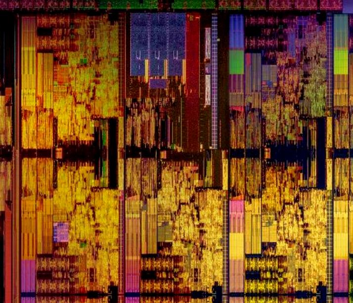
Here’s the diagram:
This is meant to be a pseudo mockup of a theoretical core of n processors using the mesh topology. At the top are the socket links, along with the PCIe root complexes. However on the left and right are the DRAM controllers, essentially taking up the same area as a core but also using one of the mesh networking links.
So scoot back to that HCC die image, and zoom in on one of those odd looking ‘cores’:
What we can see is three regular blue/green vertical areas, which means three on each side, for a total of six. Skylake-X only has four memory channels, but leaks have shown that the new Skylake-SP processors have six memory channels by design, so here they are. In the 4x5 grid, we have 18 cores and two sets of memory channels.
Back when Skylake-X was announced at Computex, I wrote that we were expecting the LCC silicon to be a 12-core design. At this time, we were still expecting Intel to use a ring-bus topology, and I mentioned before, adding two cores to a ring bus is fairly easy at the expense of peak latency between cores. Now that we know that Intel is using a mesh, it is quite different.
12 cores could quite easily fit into LCC silicon in a 3x4 arrangement, but that does not leave any room for the six memory controllers that the enterprise Xeons are all meant to have. If we added two ‘extra’ core sized areas for the 12-core design, we need a total of 14 segments. Using the x*y arrangement as required above, the only way 14 cores works is using a 7*2 arrangement. If this was the case, the DRAM controllers would essentially fill a whole row, or be at opposite ends of the column. If one of the x*y numbers is the number two, it makes more sense to use a ring bus any day of the week for power, die area and simplicity.
So that means that the 12-core SKU, the Core i9-7920X, is likely derived from the HCC 18-core silicon. Which also explains why that CPU has been delayed until August.
Die Sizes
At this point in time, the Skylake-X processors based on the LCC silicon have been in the hands of a few people. At Computex there were several extreme overclocking (using sub-zero coolants) events dedicated to the new processors. One element of recent extreme overclocking is delidding the processor and removing the integrated heat spreader to replace the thermal interface material underneath.
In general removing the IHS is not recommended without practice and experience, but for some processors in the past we have seen sizeable temperature benefits by replacing the standard thermal interface material (TIM) that Intel uses. The discussion on whether Intel should be offering a standard goopy TIM or the indium-tin solder that they used to (and AMD uses) is one I’ve run on AnandTech before, but there’s a really good guide from Roman Hartung, who overclocks by the name der8auer. I’m trying to get him to agree to post it on AnandTech with SKL-X updates so we can discuss it here, but it really is some nice research. You can find the guide over at http://overclocking.guide.
However removing the IHS means we can measure the silicon die.
The 10-core LCC die, which is a 3x4 design, measures in at 14.3 x 22.4, or 322mm2.
Using this, working from Intel’s 4x5 HCC diagram (and assuming it hasn’t been stretched), we can get 21.6 x 22.4 = 484mm2 for the high-core count design.
That leaves the Extreme core count option. Using the x*y strategy again, Intel could either run a 5x5 design, which gives 25 areas and 23 cores – which is unlikely. Next up is a 5x6 design, which gives 30 areas and 28 cores. It’s no secret that many leaks are pointing to a 28-core XCC processor at this point.
There’s also the fact that Intel provided this die shot at the Intel Manufacturing Day a few weeks ago, clearly showing the 5x6 arrangement:
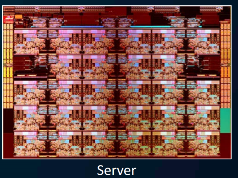
Doing the basic math on a 5x6 design gives us a 21.6 x 32.3 = 698mm2 die size for XCC.
| Skylake-SP Die Sizes | |||
| Arrangement | Dimensions (mm) |
Die Area (mm2) |
|
| LCC | 3x4 (10-core) | 14.3 x 22.4 | 322 mm2 |
| HCC | 4x5 (18-core) | 21.6 x 22.4 | 484 mm2 |
| XCC | 5x6 (28-core) | 21.6 x 32.3 | 698 mm2 |
Compared to other chips with Intel’s mesh architecture, Knights Landing comes in at 646mm2 (minus MCDRAM), and sources put Knights Corner at 720mm2.
Favored Core
For Broadwell-E, the last generation of Intel’s HEDT platform, we were introduced to the term ‘Favored Core’, which was given the title of Turbo Boost Max 3.0. The idea here is that each piece of silicon that comes off of the production line is different (which is then binned to match to a SKU), but within a piece of silicon the cores themselves will have different frequency and voltage characteristics. The one core that is determined to be the best is called the ‘Favored Core’, and when Intel’s Windows 10 driver and software were in place, single threaded workloads were moved to this favored core to run faster.
In theory, it was good – a step above the generic Turbo Boost 2.0 and offered an extra 100-200 MHz for single threaded applications. In practice, it was flawed: motherboard manufacturers didn’t support it, or they had it disabled in the BIOS by default. Users had to install the drivers and software as well – without the combination of all of these at work, the favored core feature didn’t work at all.
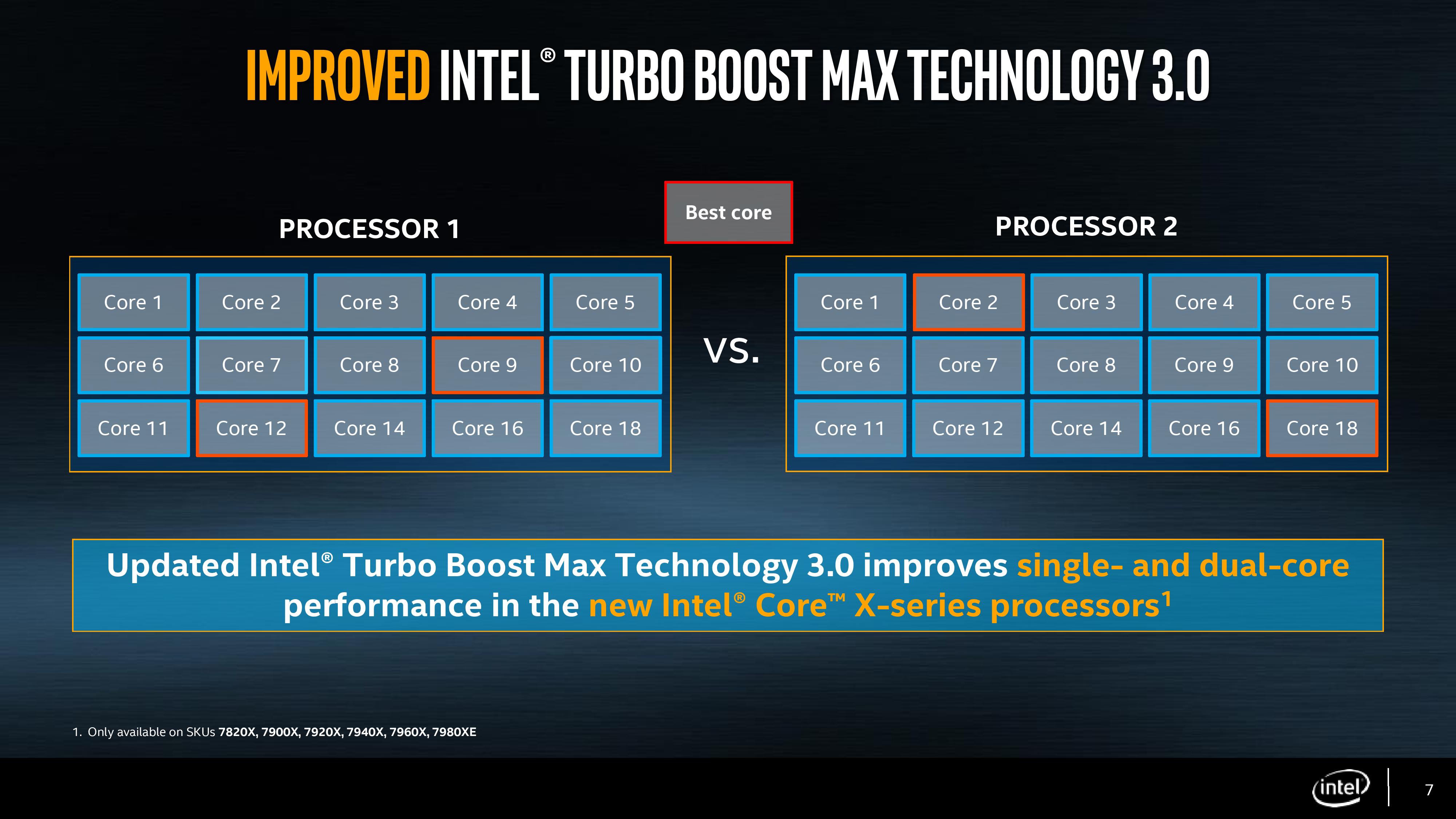
Intel is changing the feature for Skylake-X, with an upgrade and for ease-of-use. The driver and software are now part of Windows updates, so users will get them automatically (if you don’t want it, you have to disable it manually). With Skylake-X, instead of one core being the favored core, there are two cores in this family. As a result, two apps can be run at the higher frequency, or one app that needs two cores can participate.
Speed Shift
In Skylake-S, the processor has been designed in a way that with the right commands, the OS can hand control of the frequency and voltage back to the processor. Intel called this technology 'Speed Shift'. We’ve discussed Speed Shift before in the Skylake architecture analysis, and it now comes to Skylake-X. One of the requirements for Speed Shift is that it requires operating system support to be able to hand over control of the processor performance to the CPU, and Intel has had to work with Microsoft in order to get this functionality enabled in Windows 10.
Compared to Speed Step / P-state transitions, Intel's new Speed Shift terminology changes the game by having the operating system relinquish some or all control of the P-States, and handing that control off to the processor. This has a couple of noticeable benefits. First, it is much faster for the processor to control the ramp up and down in frequency, compared to OS control. Second, the processor has much finer control over its states, allowing it to choose the most optimum performance level for a given task, and therefore using less energy as a result. Specific jumps in frequency are reduced to around 1ms with Speed Shift's CPU control from 20-30 ms on OS control, and going from an efficient power state to maximum performance can be done in around 35 ms, compared to around 100 ms with the legacy implementation. As seen in the images below, neither technology can jump from low to high instantly, because to maintain data coherency through frequency/voltage changes there is an element of gradient as data is realigned.

The ability to quickly ramp up performance is done to increase overall responsiveness of the system, rather than linger at lower frequencies waiting for OS to pass commands through a translation layer. Speed Shift cannot increase absolute maximum performance, but on short workloads that require a brief burst of performance, it can make a big difference in how quickly that task gets done. Ultimately, much of what we do falls more into this category, such as web browsing or office work. As an example, web browsing is all about getting the page loaded quickly, and then getting the processor back down to idle.
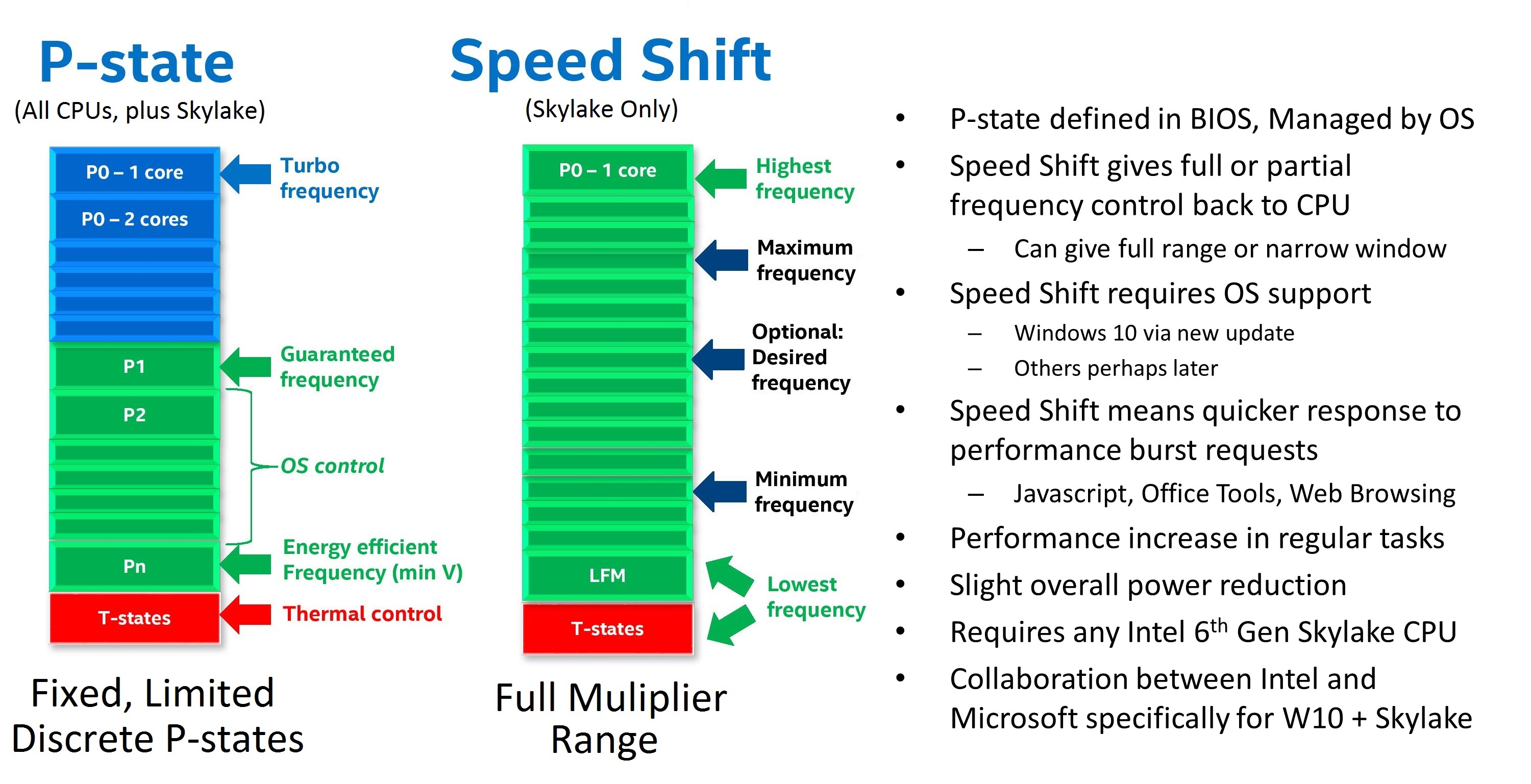
Again, Speed Shift is something that needs to be enabled on all levels - CPU, OS, driver, and motherboard BIOS. It has come to light that some motherboard manufacturers are disabling Speed Shift on desktops by default, negating the feature. In the BIOS is it labeled either as Speed Shift or Hardware P-States, and sometimes even has non-descript options. Unfortunately, a combination of this and other issues has led to a small problem on X299 motherboards.
X299 Motherboards
When we started testing for this review, the main instructions we were given was that when changing between Skylake-X and Kaby Lake-X processors, be sure to remove AC power and hold the reset BIOS button for 30 seconds. This comes down to an issue with supporting both sets of CPUs at once: Skylake-X features some form of integrated voltage regulator (somewhat like the FIVR on Broadwell), whereas Kaby Lake-X is more motherboard controlled. As a result, some of the voltages going in to the CPU, if configured incorrectly, can cause damage. This is where I say I broke a CPU: our Kaby Lake-X Core i7 died on the test bed. We are told that in the future there should be a way to switch between the two without having this issue, but there are some other issues as well.
After speaking with a number of journalists in my close circle, it was clear that some of the GPU testing was not reflective of where the processors sat in the product stack. Some results were 25-50% worse than we expected for Skylake-X (Kaby Lake-X seemingly unaffected), scoring disastrously low frame rates. This was worrying.
Speaking with the motherboard manufacturers, it's coming down to a few issues: managing the mesh frequency (and if the mesh frequency has a turbo), controlling turbo modes, and controlling features like Speed Shift. 'Controlling' in this case can mean boosting voltages to support it better, overriding the default behavior for 'performance' which works on some tests but not others, or disabling the feature completely.
We were still getting new BIOSes two days before launch, right when I need to fly half-way across the world to cover other events. Even retesting the latest BIOS we had for the boards we had, there still seems to be an underlying issue with either the games or the power management involved. This isn't necessarily a code optimization issue for the games themselves: the base microarchitecture on the CPU is still the same with a slight cache adjustment, so if a Skylake-X starts performing below an old Sandy Bridge Core i3, it's not on the game.
We're still waiting to hear for BIOS updates, or reasons why this is the case. Some games are affected a lot, others not at all. Any game we are testing which ends up being GPU limited is unaffected, showing that this is a CPU issue.
Power Consumption
Adding cores and increasing the frequency is going to have an effect on power consumption. Even though Skylake-X is built on a very competitive 14nm process, physics are physics and the best way to mitigate that is through innovative design. Ultimately here we would normally be expecting a similar result to Skylake-S, but with the new cache, mesh and AVX512 instructions, their effect on the power consumption might end up increasing power.
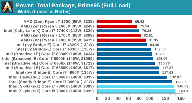
So this is surprising. Normally Intel are relatively good at their recommended TDP numbers: the ability to remove a certain amount of heat related to power consumption is something Intel either gets bang on, or has plenty of headroom. The sole Kaby Lake-X CPU that completed this test is an example: at under 60W, it is comfortably under the 112W TDP that chip has. But for the 140W Skylake-X parts, we recorded nearly 150W power consumption. Intel announced that the socket is suitable up to 165W, so it’s clear that they are pushing the frequencies here and it is going to be telling what might happen with the higher core count silicon.
Test Bed and Setup
As per our processor testing policy, we take a premium category motherboard suitable for the socket, and equip the system with a suitable amount of memory running at the manufacturer's maximum supported frequency. This is also typically run at JEDEC subtimings where possible. It is noted that some users are not keen on this policy, stating that sometimes the maximum supported frequency is quite low, or faster memory is available at a similar price, or that the JEDEC speeds can be prohibitive for performance. While these comments make sense, ultimately very few users apply memory profiles (either XMP or other) as they require interaction with the BIOS, and most users will fall back on JEDEC supported speeds - this includes home users as well as industry who might want to shave off a cent or two from the cost or stay within the margins set by the manufacturer. Where possible, we will extend out testing to include faster memory modules either at the same time as the review or a later date.
| Test Setup | |
| Processor | Intel Core i9-7900X (10C/20T, 140W, 3.3 GHz) Intel Core i7-7820X (8C/20T, 140W, 3.6 GHz) Intel Core i7-7800X (6C/12T, 140W, 3.5 GHz) Intel Core i7-7740X (4C/8T, 112W, 4.3 GHz) Intel Core i5-7640X (4C/4T, 112W, 4.0 GHz) |
| Motherboards | ASRock X299 Taichi MSI X299 Gaming Pro Carbon GIGABYTE X299 Gaming 9 |
| Cooling | Thermalright TRUE Copper Silverstone AR10-115XS |
| Power Supply | Corsair AX760i PSU Corsair AX1200i Platinum PSU |
| Memory | Corsair Vengeance Pro DDR4-2666 4x8 GB or G.Skill Ripjaws 4 DDR4-2666 C15 4x8GB or TeamGroup NightHawk RGB DDR4-3000 |
| Video Cards | MSI GTX 1080 Gaming 8GB ASUS GTX 1060 Strix Sapphire R9 Fury 4GB Sapphire RX 480 8GB Sapphire RX 460 2GB |
| Hard Drive | Crucial MX200 1TB |
| Optical Drive | LG GH22NS50 |
| Case | Open Test Bed |
| Operating System | Windows 10 Pro 64-bit |
Many thanks to...
We must thank the following companies for kindly providing hardware for our multiple test beds. Some of this hardware is not in this test bed specifically, but is used in other testing.
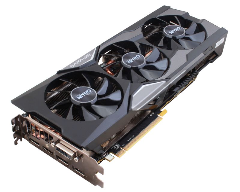
Thank you to Sapphire for providing us with several of their AMD GPUs. We met with Sapphire back at Computex 2016 and discussed a platform for our future testing on AMD GPUs with their hardware for several upcoming projects. As a result, they were able to sample us the latest silicon that AMD has to offer. At the top of the list was a pair of Sapphire Nitro R9 Fury 4GB GPUs, based on the first generation of HBM technology and AMD’s Fiji platform. As the first consumer GPU to use HDM, the R9 Fury is a key moment in graphics history, and this Nitro cards come with 3584 SPs running at 1050 MHz on the GPU with 4GB of 4096-bit HBM memory at 1000 MHz.
Further Reading: AnandTech’s Sapphire Nitro R9 Fury Review
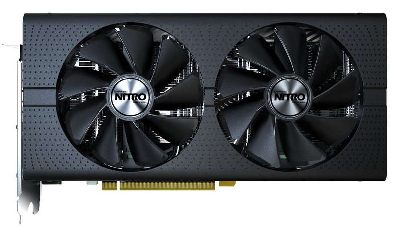
Following the Fury, Sapphire also supplied a pair of their latest Nitro RX 480 8GB cards to represent AMD’s current performance silicon on 14nm (as of March 2017). The move to 14nm yielded significant power consumption improvements for AMD, which combined with the latest version of GCN helped bring the target of a VR-ready graphics card as close to $200 as possible. The Sapphire Nitro RX 480 8GB OC graphics card is designed to be a premium member of the RX 480 family, having a full set of 8GB of GDDR5 memory at 6 Gbps with 2304 SPs at 1208/1342 MHz engine clocks.
Further Reading: AnandTech’s AMD RX 480 Review
With the R9 Fury and RX 480 assigned to our gaming tests, Sapphire also passed on a pair of RX 460s to be used as our CPU testing cards. The amount of GPU power available can have a direct effect on CPU performance, especially if the CPU has to spend all its time dealing with the GPU display. The RX 460 is a nice card to have here, as it is powerful yet low on power consumption and does not require any additional power connectors. The Sapphire Nitro RX 460 2GB still follows on from the Nitro philosophy, and in this case is designed to provide power at a low price point. Its 896 SPs run at 1090/1216 MHz frequencies, and it is paired with 2GB of GDDR5 at an effective 7000 MHz.

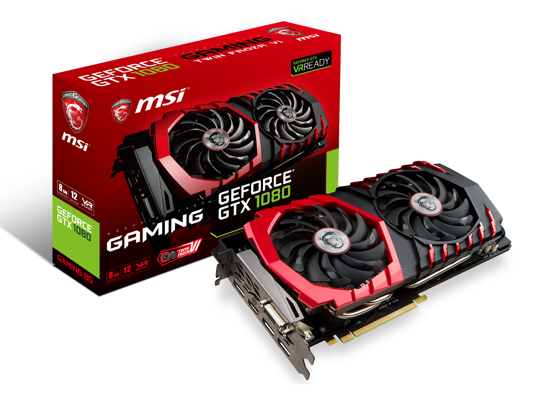
We must also say thank you to MSI for providing us with their GTX 1080 Gaming X 8GB GPUs. Despite the size of AnandTech, securing high-end graphics cards for CPU gaming tests is rather difficult. MSI stepped up to the plate in good fashion and high spirits with a pair of their high-end graphics. The MSI GTX 1080 Gaming X 8GB graphics card is their premium air cooled product, sitting below the water cooled Seahawk but above the Aero and Armor versions. The card is large with twin Torx fans, a custom PCB design, Zero-Frozr technology, enhanced PWM and a big backplate to assist with cooling. The card uses a GP104-400 silicon die from a 16nm TSMC process, contains 2560 CUDA cores, and can run up to 1847 MHz in OC mode (or 1607-1733 MHz in Silent mode). The memory interface is 8GB of GDDR5X, running at 10010 MHz. For a good amount of time, the GTX 1080 was the card at the king of the hill.
Further Reading: AnandTech’s NVIDIA GTX 1080 Founders Edition Review
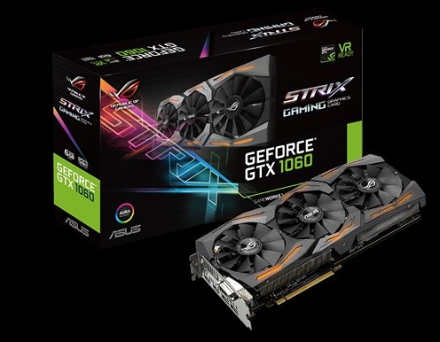
Thank you to ASUS for providing us with their GTX 1060 6GB Strix GPU. To complete the high/low cases for both AMD and NVIDIA GPUs, we looked towards the GTX 1060 6GB cards to balance price and performance while giving a hefty crack at >1080p gaming in a single graphics card. ASUS lended a hand here, supplying a Strix variant of the GTX 1060. This card is even longer than our GTX 1080, with three fans and LEDs crammed under the hood. STRIX is now ASUS’ lower cost gaming brand behind ROG, and the Strix 1060 sits at nearly half a 1080, with 1280 CUDA cores but running at 1506 MHz base frequency up to 1746 MHz in OC mode. The 6 GB of GDDR5 runs at a healthy 8008 MHz across a 192-bit memory interface.
Further Reading: AnandTech’s ASUS GTX 1060 6GB STRIX Review
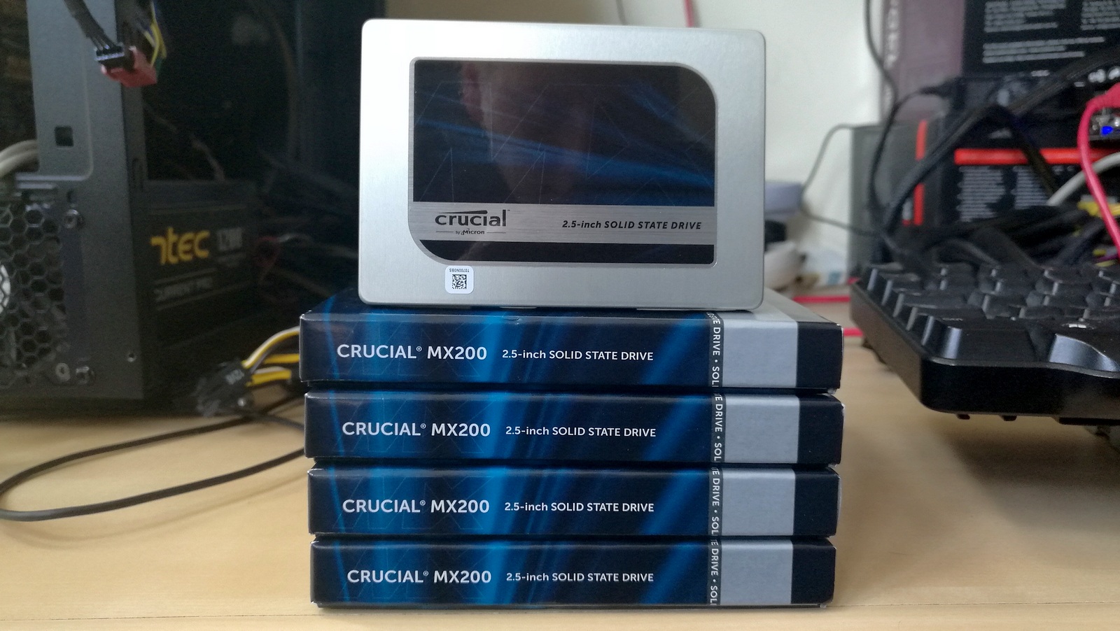
Thank you to Crucial for providing us with MX200 SSDs. Crucial stepped up to the plate as our benchmark list grows larger with newer benchmarks and titles, and the 1TB MX200 units are strong performers. Based on Marvell's 88SS9189 controller and using Micron's 16nm 128Gbit MLC flash, these are 7mm high, 2.5-inch drives rated for 100K random read IOPs and 555/500 MB/s sequential read and write speeds. The 1TB models we are using here support TCG Opal 2.0 and IEEE-1667 (eDrive) encryption and have a 320TB rated endurance with a three-year warranty.
Further Reading: AnandTech's Crucial MX200 (250 GB, 500 GB & 1TB) Review
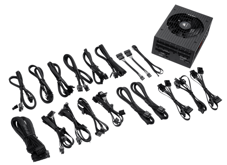
Thank you to Corsair for providing us with AX760i and AX1200i PSUs. The AX1200i was the first power supply to offer digital control and management via Corsair's Link system, but under the hood it commands a 1200W rating at 50C with 80 PLUS Platinum certification. This allows for a minimum 89-92% efficiency at 115V and 90-94% at 230V. The AX1200i is completely modular, running the larger 200mm design, with a dual ball bearing 140mm fan to assist high-performance use. The AX1200i is designed to be a workhorse, with up to 8 PCIe connectors for suitable four-way GPU setups. The AX1200i also comes with a Zero RPM mode for the fan, which due to the design allows the fan to be switched off when the power supply is under 30% load.
Further Reading: AnandTech's Corsair AX1500i Power Supply Review
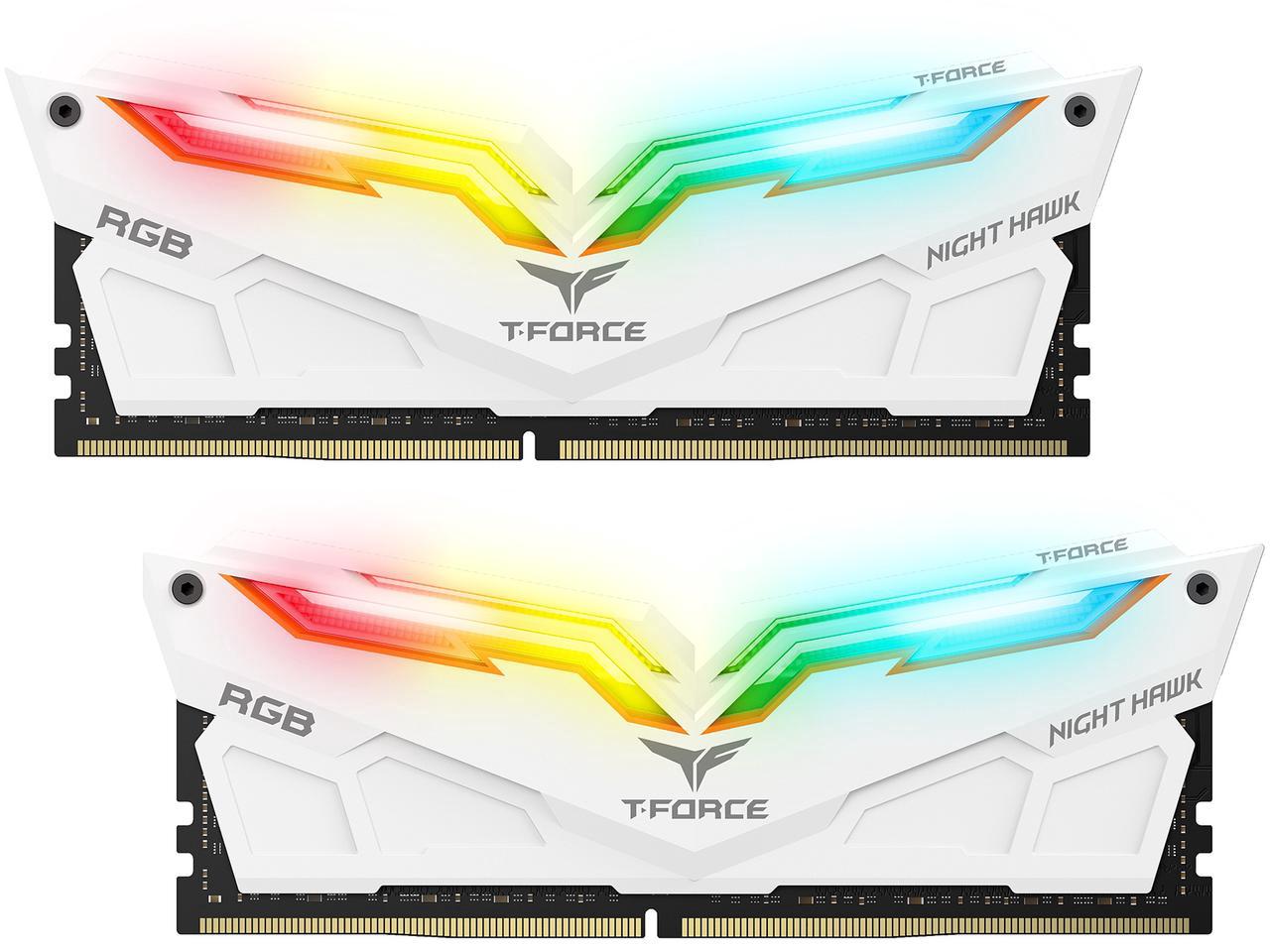
Thank you to TeamGroup for providing us with Nighthawk RGB Memory.
Benchmarking Suite 2017
2017 CPU
For our review, we are implementing our fresh CPU testing benchmark suite, using new scripts developed specifically for this testing. This means that with a fresh OS install, we can configure the OS to be more consistent, install the new benchmarks, maintain version consistency without random updates and start running the tests in under 5 minutes. After that it's a one button press to start an 8-10hr test (with a high-performance core) with nearly 100 relevant data points in the benchmarks given below. The tests cover a wide range of segments, some of which will be familiar but some of the tests are new to benchmarking in general, but still highly relevant for the markets they come from.
Our new CPU tests go through six main areas. We cover the Web (we've got an un-updateable version of Chrome 56), general system tests (opening tricky PDFs, emulation, brain simulation, AI, 2D image to 3D model conversion), rendering (ray tracing, modeling), encoding (compression, AES, h264 and HEVC), office based tests (PCMark and others), and our legacy tests, throwbacks from another generation of bad code but interesting to compare.
A side note on OS preparation. As we're using Windows 10, there's a large opportunity for something to come in and disrupt our testing. So our default strategy is multiple: disable the ability to update as much as possible, disable Windows Defender, uninstall OneDrive, disable Cortana as much as possible, implement the high performance mode in the power options, and disable the internal platform clock which can drift away from being accurate if the base frequency drifts (and thus the timing ends up inaccurate).
Web Tests on Chrome 56
Sunspider
Kraken
Octane
Web13
Web15
System Tests
PDF Opening
FCAT
3DPM v21
Dolphin v5.0
DigiCortex v1.20
Agisoft PS v1.0
Rendering Tests
Corona 1.3
Blender 2.78
LuxMark CPU C++
LuxMark CPU OpenCL
POV-Ray
CB15 ST
CB15 MT
Encoding Tests
7-Zip
WinRAR 5.4
TrueCrypt
HandBrake 264-LQ
HandBrake 264-HQ
HandBrake 265-4K
Office / Professional
PCMark8
Chromium Compile
SYSmark 2014 SE
Legacy Tests
3DPM v1 ST / MT
x264 HD 3 Pass 1, Pass 2
CB 11.5 ST / MT
CB 10 ST / MT
A side note - a couple of benchmarks (LuxMark) weren't fully 100% giving good data during testing. Need to go back and re-work this part of our testing.
2017 GPU
For our 2017 set of GPU tests, we wanted to think big. There are a lot of users in the ecosystem that prioritize gaming above all else, especially when it comes to choosing the correct CPU. If there's a chance to save $50 and get a better graphics card for no loss in performance, then this is the route that gamers would prefer to tread. The angle here though is tough - lots of games have different requirements and cause different stresses on a system, with various graphics cards having different reactions to the code flow of a game. Then users also have different resolutions and different perceptions of what feels 'normal'. This all amounts to more degrees of freedom than we could hope to test in a lifetime, only for the data to become irrelevant in a few months when a new game or new GPU comes into the mix. Just for good measure, let us add in DirectX 12 titles that make it easier to use more CPU cores in a game to enhance fidelity.
Our original list of nine games planned in February quickly became six, due to the lack of professional-grade controls on Ubisoft titles. If you want to see For Honor, Steep or Ghost Recon: Wildlands benchmarked on AnandTech, point Ubisoft Annecy or Ubisoft Montreal in my direction. While these games have in-game benchmarks worth using, unfortunately they do not provide enough frame-by-frame detail to the end user, despite using it internally to produce the data the user eventually sees (and it typically ends up obfuscated by another layer as well). I would instead perhaps choose to automate these benchmarks via inputs, however the extremely variable loading time is a strong barrier to this.
So we have the following benchmarks as part of our 4/2 script, automated to the point of a one-button run and out pops the results four hours later, per GPU. Also listed are the resolutions and settings used.
- Civilization 6 (1080p Ultra, 4K Ultra)
- Ashes of the Singularity: Escalation* (1080p Extreme, 4K Extreme)
- Shadow of Mordor (1080p Ultra, 4K Ultra)
- Rise of the Tomb Raider #1 - GeoValley (1080p High, 4K Medium)
- Rise of the Tomb Raider #2 - Prophets (1080p High, 4K Medium)
- Rise of the Tomb Raider #3 - Mountain (1080p High, 4K Medium)
- Rocket League (1080p Ultra, 4K Ultra)
- Grand Theft Auto V (1080p Very High, 4K High)
For each of the GPUs in our testing, these games (at each resolution/setting combination) are run four times each, with outliers discarded. Average frame rates, 99th percentiles and 'Time Under x FPS' data is sorted, and the raw data is archived.
The four GPUs we've managed to obtain for these tests are:
- MSI GTX 1080 Gaming X 8G
- ASUS GTX 1060 Strix 6G
- Sapphire Nitro R9 Fury 4GB
- Sapphire Nitro RX 480 8GB
In our testing script, we save a special thing for the GTX 1080 here. The following tests are also added:
- Civilization 6 (8K Ultra, 16K Lowest)
These two benchmarks, with a little coercion, are able to be run beyond the specifications of the monitor being used, allowing for 'future' testing of GPUs at 8K and 16K with some amusing results. We are only running these tests on the GTX 1080, because there's no point watching a slideshow more than once.
*A note on Ashes. During our initial testing, 8K and 16K testing were working great. But a game update around v.2.2 broke our scripting methods due to a new splashscreen/popup. We worked to find a solution that worked in order to start testing, however it still remains a kludge and the new resolution testing system stopped working. If it ever works again, we might start testing in 8K/16K.
Benchmarking Performance: CPU System Tests
Our first set of tests is our general system tests. These set of tests are meant to emulate more about what people usually do on a system, like opening large files or processing small stacks of data. This is a bit different to our office testing, which uses more industry standard benchmarks, and a few of the benchmarks here are relatively new and different.
PDF Opening
First up is a self-penned test using a monstrous PDF we once received in advance of attending an event. While the PDF was only a single page, it had so many high-quality layers embedded it was taking north of 15 seconds to open and to gain control on the mid-range notebook I was using at the time. This put it as a great candidate for our 'let's open an obnoxious PDF' test. Here we use Adobe Reader DC, and disable all the update functionality within. The benchmark sets the screen to 1080p, opens the PDF to in fit-to-screen mode, and measures the time from sending the command to open the PDF until it is fully displayed and the user can take control of the software again. The test is repeated ten times, and the average time taken. Results are in milliseconds.
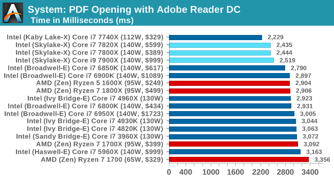
The extra frequency of the new processors is helping when it comes to opening our monster PDF, but also the extra L2 cache is likely having an effect as well.
FCAT Processing
One of the more interesting workloads that has crossed our desks in recent quarters is FCAT - the tool we use to measure stuttering in gaming due to dropped or runt frames. The FCAT process requires enabling a color-based overlay onto a game, recording the gameplay, and then parsing the video file through the analysis software. The software is mostly single-threaded, however because the video is basically in a raw format, the file size is large and requires moving a lot of data around. For our test, we take a 90-second clip of the Rise of the Tomb Raider benchmark running on a GTX 980 Ti at 1440p, which comes in around 21 GB, and measure the time it takes to process through the visual analysis tool.
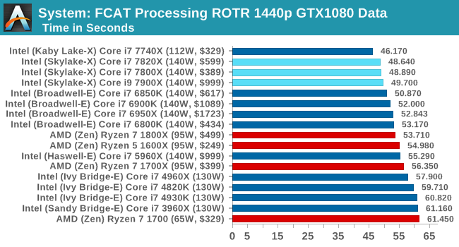
FCAT takes in a frame, processes it and dumps it, all on a single thread. The quicker you get through the workload the better, and frequency is supreme, hence we get the 7820X followed by the 7800X then the 7900X. Even though the 7900X has the higher turbo here, the results are with the margin expected.
3D Particle Movement v2.1
This is the latest version of the self-penned 3DPM benchmark. The goal of 3DPM is to simulate semi-optimized scientific algorithms taken directly from my doctorate thesis. Version 2.1 improves over 2.0 by passing the main particle structs by reference rather than by value, and decreasing the amount of double->float->double recasts the compiler was adding in. It affords a ~25% speed-up over v2.0, which means new data.
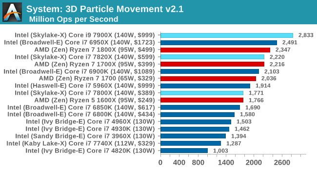
Give 3DPMv2.1 some cores, and it will show you the world / some numbers. The 1800X and 6950X were gunning for top spot, but the extra frequency of the 7900X wins here.
DigiCortex 1.20
Despite being a couple of years old, the DigiCortex software is a pet project for the visualization of neuron and synapse activity in the brain. The software comes with a variety of benchmark modes, and we take the small benchmark which runs a 32k neuron/1.8B synapse simulation. The results on the output are given as a fraction of whether the system can simulate in real-time, so anything above a value of one is suitable for real-time work. The benchmark offers a 'no firing synapse' mode, which in essence detects DRAM and bus speed, however we take the firing mode which adds CPU work with every firing.
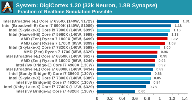
DigiCortex loves a bit of memory, although when speaking with the developer, there can some instances where the beast needs to be fed. Losing the inclusive L3 might be a factor here, especially with the 7800X all the way down.
Agisoft Photoscan 1.0
Photoscan stays in our benchmark suite from the previous version, however now we are running on Windows 10 so features such as Speed Shift on the latest processors come into play. The concept of Photoscan is translating many 2D images into a 3D model - so the more detailed the images, and the more you have, the better the model. The algorithm has four stages, some single threaded and some multi-threaded, along with some cache/memory dependency in there as well. For some of the more variable threaded workload, features such as Speed Shift and XFR will be able to take advantage of CPU stalls or downtime, giving sizeable speedups on newer microarchitectures.
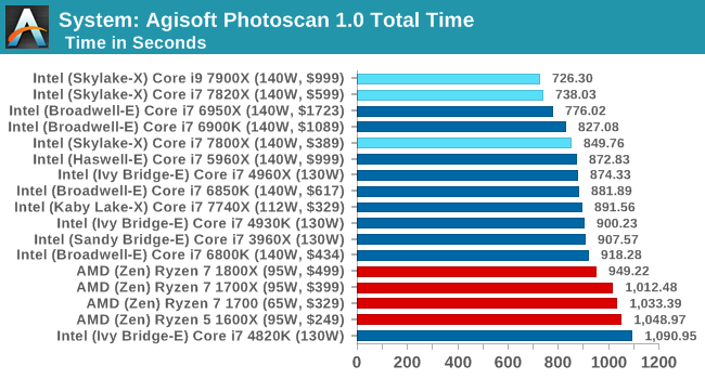
Photoscan is a mixed bag of operations, going through single thread sections to multithread and a range of cache/memory bandwidth requirepements. There's not much difference between thw 10 core and the 8 core, but the frequency helps against Broadwell-E.
Benchmarking Performance: CPU Rendering Tests
Rendering tests are a long-time favorite of reviewers and benchmarkers, as the code used by rendering packages is usually highly optimized to squeeze every little bit of performance out. Sometimes rendering programs end up being heavily memory dependent as well - when you have that many threads flying about with a ton of data, having low latency memory can be key to everything. Here we take a few of the usual rendering packages under Windows 10, as well as a few new interesting benchmarks.
Corona 1.3
Corona is a standalone package designed to assist software like 3ds Max and Maya with photorealism via ray tracing. It's simple - shoot rays, get pixels. OK, it's more complicated than that, but the benchmark renders a fixed scene six times and offers results in terms of time and rays per second. The official benchmark tables list user submitted results in terms of time, however I feel rays per second is a better metric (in general, scores where higher is better seem to be easier to explain anyway). Corona likes to pile on the threads, so the results end up being very staggered based on thread count.
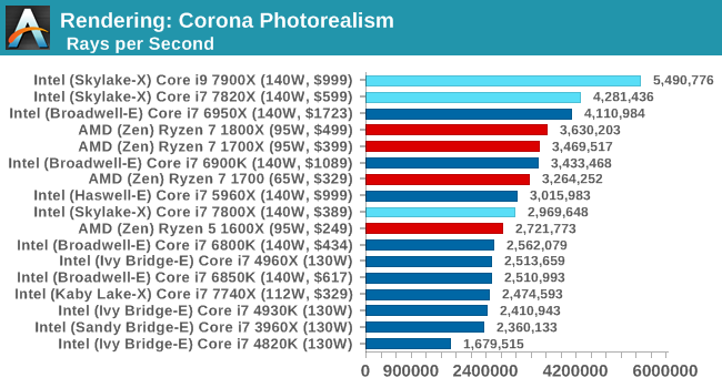
Blender 2.78
For a render that has been around for what seems like ages, Blender is still a highly popular tool. We managed to wrap up a standard workload into the February 5 nightly build of Blender and measure the time it takes to render the first frame of the scene. Being one of the bigger open source tools out there, it means both AMD and Intel work actively to help improve the codebase, for better or for worse on their own/each other's microarchitecture.
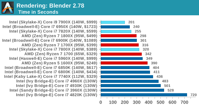
LuxMark
As a synthetic, LuxMark might come across as somewhat arbitrary as a renderer, given that it's mainly used to test GPUs, but it does offer both an OpenCL and a standard C++ mode. In this instance, aside from seeing the comparison in each coding mode for cores and IPC, we also get to see the difference in performance moving from a C++ based code-stack to an OpenCL one with a CPU as the main host.
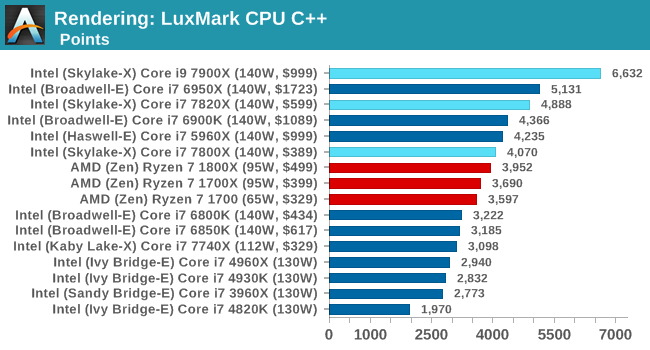
POV-Ray 3.7b3
Another regular benchmark in most suites, POV-Ray is another ray-tracer but has been around for many years. It just so happens that during the run up to AMD's Ryzen launch, the code base started to get active again with developers making changes to the code and pushing out updates. Our version and benchmarking started just before that was happening, but given time we will see where the POV-Ray code ends up and adjust in due course.
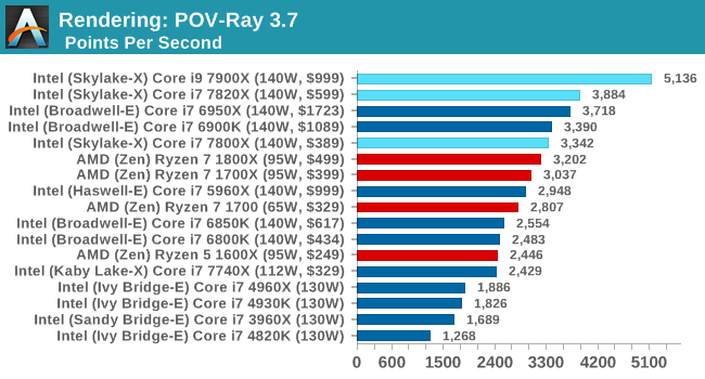
Cinebench R15
The latest version of CineBench has also become one of those 'used everywhere' benchmarks, particularly as an indicator of single thread performance. High IPC and high frequency gives performance in ST, whereas having good scaling and many cores is where the MT test wins out.
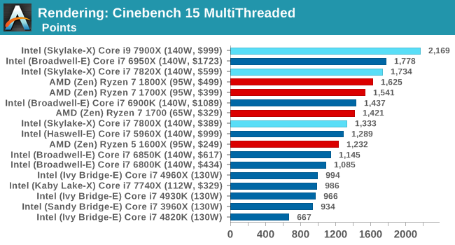
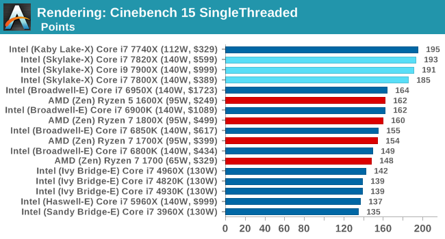
Benchmarking Performance: CPU Web Tests
One of the issues when running web-based tests is the nature of modern browsers to automatically install updates. This means any sustained period of benchmarking will invariably fall foul of the 'it's updated beyond the state of comparison' rule, especially when browsers will update if you give them half a second to think about it. Despite this, we were able to find a series of commands to create an un-updatable version of Chrome 56 for our 2017 test suite. While this means we might not be on the bleeding edge of the latest browser, it makes the scores between CPUs comparable.
SunSpider 1.0.2
The oldest web-based benchmark in this portion of our test is SunSpider. This is a very basic javascript algorithm tool, and ends up being more a measure of IPC and latency than anything else, with most high-performance CPUs scoring around about the same. The basic test is looped 10 times and the average taken. We run the basic test 4 times.
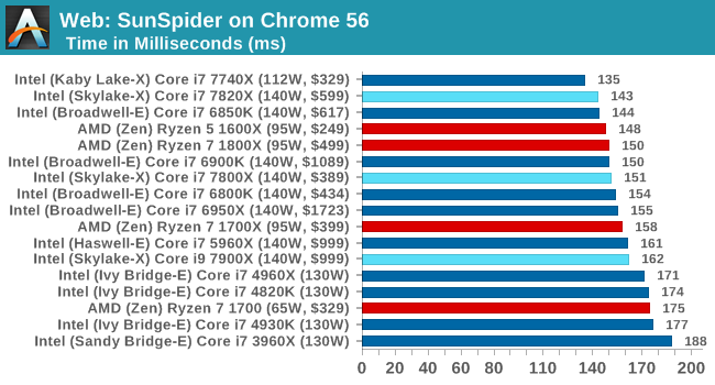
Sunspider goes after peak frequency most of the time, althoguh there is some variation as it moves into basically becoming a legacy test.
Mozilla Kraken 1.1
Kraken is another Javascript based benchmark, using the same test harness as SunSpider, but focusing on more stringent real-world use cases and libraries, such as audio processing and image filters. Again, the basic test is looped ten times, and we run the basic test four times.
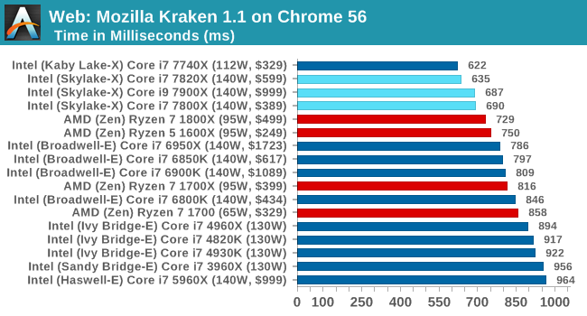
Kraken is more of an intense attack on JS, and still regularly sorts by IPC and frequency.
Google Octane 2.0
Along with Mozilla, as Google is a major browser developer, having peak JS performance is typically a critical asset when comparing against the other OS developers. In the same way that SunSpider is a very early JS benchmark, and Kraken is a bit newer, Octane aims to be more relevant to real workloads, especially in power constrained devices such as smartphones and tablets.
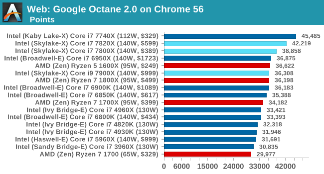
Octane seems to be an optimization target, and with the new Skylake-X it shows.
WebXPRT 2015
While the previous three benchmarks do calculations in the background and represent a score, WebXPRT is designed to be a better interpretation of visual workloads that a professional user might have, such as browser based applications, graphing, image editing, sort/analysis, scientific analysis and financial tools.
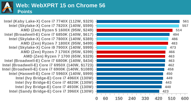
Benchmarking Performance: CPU Encoding Tests
One of the interesting elements on modern processors is encoding performance. This includes encryption/decryption, as well as video transcoding from one video format to another. In the encrypt/decrypt scenario, this remains pertinent to on-the-fly encryption of sensitive data - a process by which more modern devices are leaning to for software security. Video transcoding as a tool to adjust the quality, file size and resolution of a video file has boomed in recent years, such as providing the optimum video for devices before consumption, or for game streamers who are wanting to upload the output from their video camera in real-time. As we move into live 3D video, this task will only get more strenuous, and it turns out that the performance of certain algorithms is a function of the input/output of the content.
HandBrake H264 and HEVC
As mentioned above, video transcoding (both encode and decode) is a hot topic in performance metrics as more and more content is being created. First consideration is the standard in which the video is encoded, which can be lossless or lossy, trade performance for file-size, trade quality for file-size, or all of the above can increase encoding rates to help accelerate decoding rates. Alongside Google's favorite codec, VP9, there are two others that are taking hold: H264, the older codec, is practically everywhere and is designed to be optimized for 1080p video, and HEVC (or H265) that is aimed to provide the same quality as H264 but at a lower file-size (or better quality for the same size). HEVC is important as 4K is streamed over the air, meaning less bits need to be transferred for the same quality content.
Handbrake is a favored tool for transcoding, and so our test regime takes care of three areas.
Low Quality/Resolution H264: He we transcode a 640x266 H264 rip of a 2 hour film, and change the encoding from Main profile to High profile, using the very-fast preset.
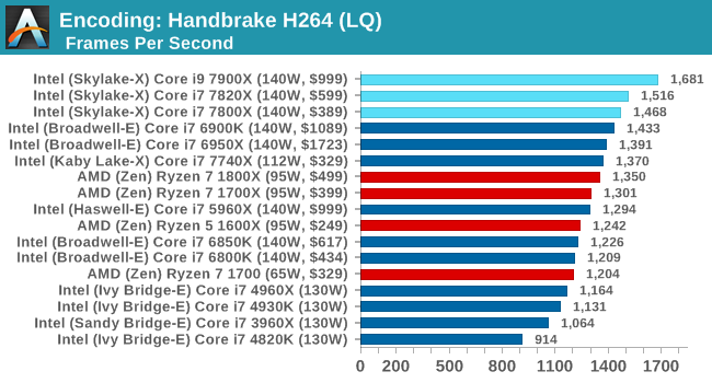
More cores, more frequency, more IPC, more fun: the Core i9-7900X wins here, and even the i7-7800X wins out against the Core i7-6900K.
High Quality/Resolution H264: A similar test, but this time we take a ten-minute double 4K (3840x4320) file running at 60 Hz and transcode from Main to High, using the very-fast preset.
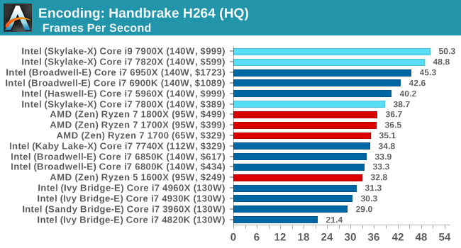
Moving into HQ mode means making the job more parallel, so the higher core counts stay at the top of the chart.
HEVC Test: Using the same video in HQ, we change the resolution and codec of the original video from 4K60 in H264 into 4K60 HEVC.
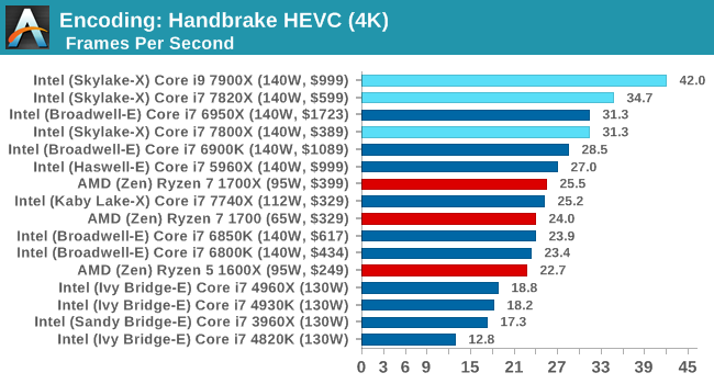
WinRAR 5.40
For the 2017 test suite, we move to the latest version of WinRAR in our compression test. WinRAR in some quarters is more user friendly that 7-Zip, hence its inclusion. Rather than use a benchmark mode as we did with 7-Zip, here we take a set of files representative of a generic stack (33 video files in 1.37 GB, 2834 smaller website files in 370 folders in 150 MB) of compressible and incompressible formats. The results shown are the time taken to encode the file. Due to DRAM caching, we run the test 10 times and take the average of the last five runs when the benchmark is in a steady state.
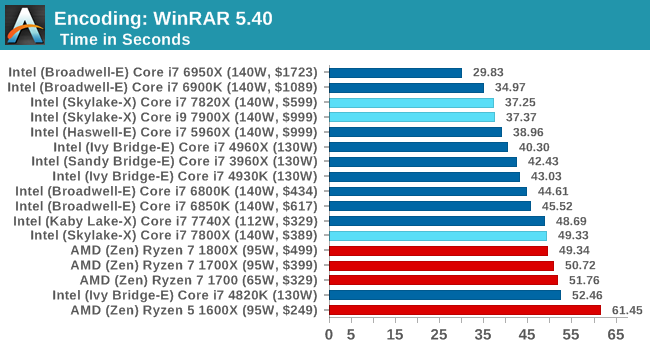
WinRAR loves having access to all the caches as much as possible, to prefetch and store data as needed. The Skylake-X chips fall back a bit here, even with DDR4-2666 support. The Core i7-7800X uses DDR4-2400 memory, so puts it further behind. Interesting didn't realise that the lower core count Broadwell-E chips were affected so much by this test, and the higher core count Ivy Bridge-E parts are faster here.
AES Encoding
Algorithms using AES coding have spread far and wide as a ubiquitous tool for encryption. Again, this is another CPU limited test, and modern CPUs have special AES pathways to accelerate their performance. We often see scaling in both frequency and cores with this benchmark. We use the latest version of TrueCrypt and run its benchmark mode over 1GB of in-DRAM data. Results shown are the GB/s average of encryption and decryption.
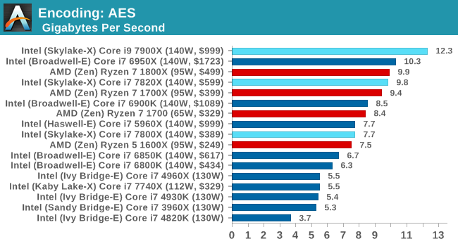
7-Zip
One of the freeware compression tools that offers good scaling performance between processors is 7-Zip. It runs under an open-source licence, is fast, and easy to use tool for power users. We run the benchmark mode via the command line for four loops and take the output score.
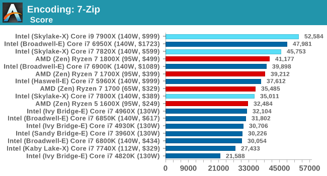
Benchmarking Performance: CPU Office Tests
The office programs we use for benchmarking aren't specific programs per-se, but industry standard tests that hold weight with professionals. The goal of these tests is to use an array of software and techniques that a typical office user might encounter, such as video conferencing, document editing, architectural modelling, and so on and so forth.
Chromium Compile (v56)
Our new compilation test uses Windows 10 Pro, VS Community 2015.3 with the Win10 SDK to combile a nightly build of Chromium. We've fixed the test for a build in late March 2017, and we run a fresh full compile in our test. Compilation is the typical example given of a variable threaded workload - some of the compile and linking is linear, whereas other parts are multithreaded.
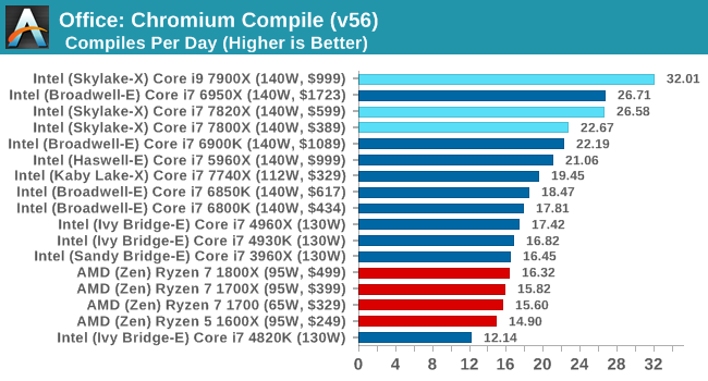
PCMark8
Despite originally coming out in 2008/2009, Futuremark has maintained PCMark8 to remain relevant in 2017. On the scale of complicated tasks, PCMark focuses more on the low-to-mid range of professional workloads, making it a good indicator for what people consider 'office' work. We run the benchmark from the commandline in 'conventional' mode, meaning C++ over OpenCL, to remove the graphics card from the equation and focus purely on the CPU. PCMark8 offers Home, Work and Creative workloads, with some software tests shared and others unique to each benchmark set.
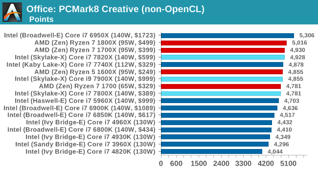
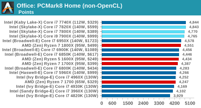
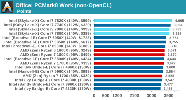
SYSmark 2014 SE
SYSmark is developed by Bapco, a consortium of industry CPU companies. The goal of SYSmark is to take stripped down versions of popular software, such as Photoshop and Onenote, and measure how long it takes to process certain tasks within that software. The end result is a score for each of the three segments (Office, Media, Data) as well as an overall score. Here a reference system (Core i3-6100, 4GB DDR3, 256GB SSD, Integrated HD 530 graphics) is used to provide a baseline score of 1000 in each test.
A note on context for these numbers. AMD left Bapco in the last two years, due to differences of opinion on how the benchmarking suites were chosen and AMD believed the tests are angled towards Intel processors and had optimizations to show bigger differences than what AMD felt was present. The following benchmarks are provided as data, but the conflict of opinion between the two companies on the validity of the benchmark is provided as context for the following numbers.
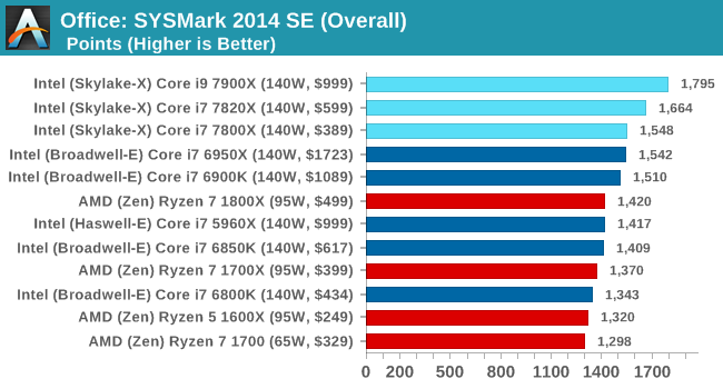
Benchmarking Performance: CPU Legacy Tests
Our legacy tests represent benchmarks that were once at the height of their time. Some of these are industry standard synthetics, and we have data going back over 10 years. All of the data here has been rerun on Windows 10, and we plan to go back several generations of components to see how performance has evolved.
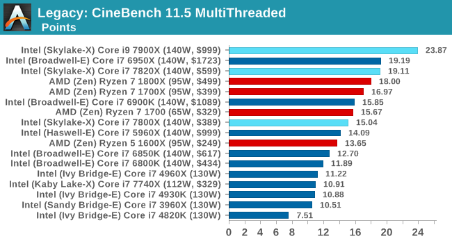
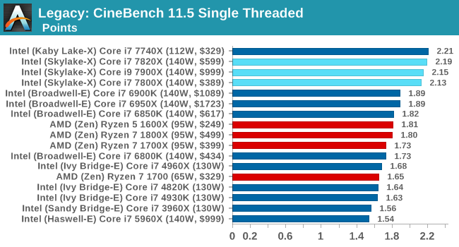
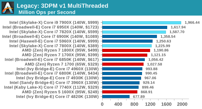
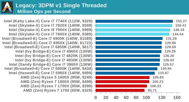
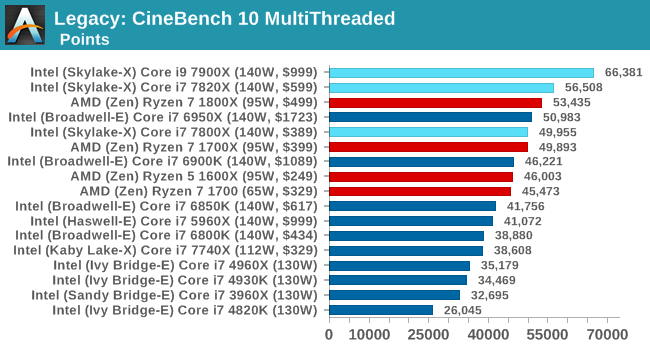
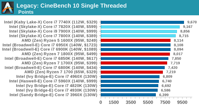
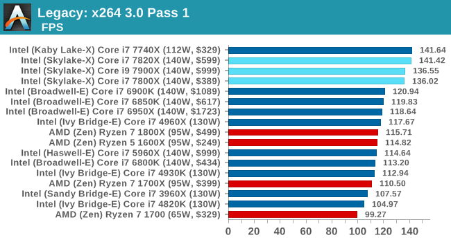
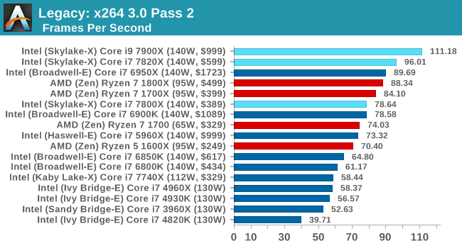
Comparing Skylake-S and Skylake-X/SP Performance Clock-for-Clock
If you’ve read through the full review up to this point (and kudos), there should be three things that stick in the back of your mind about the new Skylake-SP cores: Cache, Mesh and AVX512. These are the three main features that separate the consumer grade Skylake-S core from this new core, and all three can have an impact in clock-for-clock performance. Even though the Skylake-S and the Skylake-SP are not competing in the same markets, it is still poignant to gather how much the changes affect the regular benchmark suite.
For this test, we took the Skylake-S based Core i5-6600 and the Skylake-SP based Core i9-7900X and ran them both with only 4 cores, no hyperthreading, and 3 GHz on all cores with no Turbo active. Both CPUs were run in high performance modes in the OS to restrict any time-to-idle, so it is worth noting here that we are not measuring power. This is just raw throughput.
Both of these cores support different DRAM frequencies, however: the i5-6600 lists DDR4-2133 as its maximum supported frequency, whereas the i9-7900X will run at DDR4-2400 at 2DPC. I queried a few colleagues as to what I should do here – technically the memory support is an extended element of the microarchitecture, and the caches/uncore/untile will be running at different frequencies, so how much of the system support should be chipped away for parity. The general consensus was to test with the supported frequencies, given this is how the parts ship.
For this analysis, each test was broken down in two ways: what sort of benchmark (single thread, multi-thread, mixed) and what category of benchmark (web, office, encode).
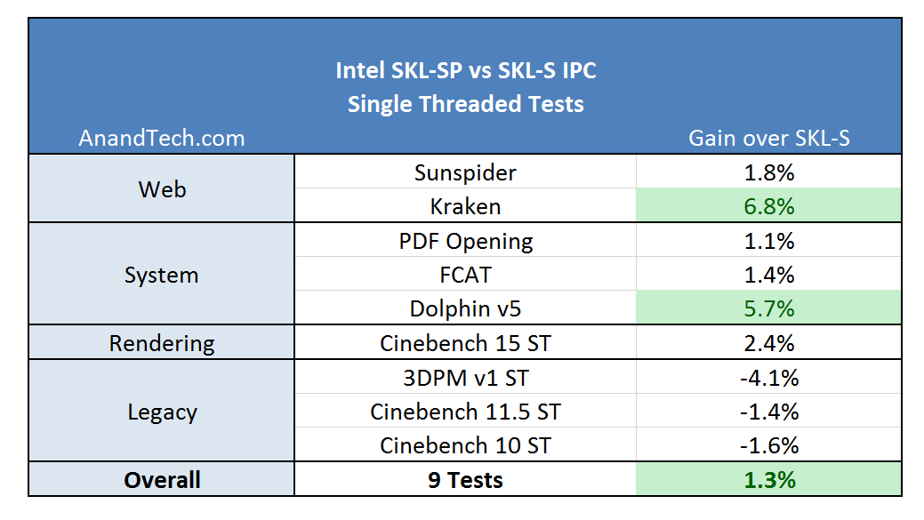
For the single threaded tests, results were generally positive. Kraken enjoyed the L2, and Dolphin emulation had a good gain as well. The legacy tests did not fair that great: 3DPM v1 has false sharing, which is likely taking a hit due to the increased L2 latency.
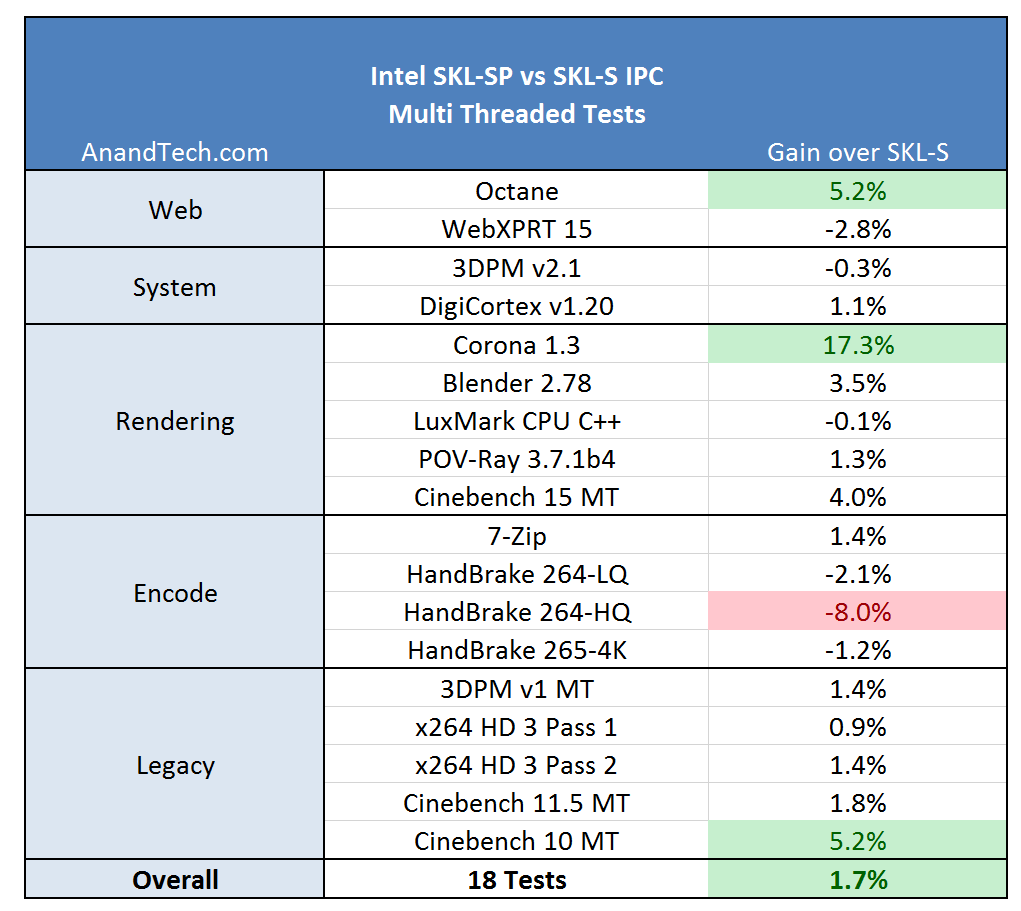
On the multithreaded tests, the big winner here was Corona. Corona is a high-performance renderer for Autodesk 3ds Max, showing that the larger L2 does a good job with its code base. The step back was in Handbrake – our testing does not implement any AVX512 code, but the L3 victim cache might be at play here over the L3 inclusive cache in SKL-S.
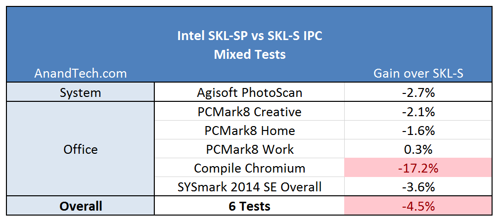
The mixed results are surprising: these tests vary with ST and MT parts to their computation, some being cache sensitive as well. The big outlier here is the compile test, indicating that the Skylake-SP might not be (clock for clock) a great compilation core. This is a result we can trace back to the L3 again, being a smaller non-inclusive cache. In our results database, we can see similar results when comparing a Ryzen 7 1700X, an 8-core 95W CPU with 16MB of L3 victim cache, is easily beaten by a Core i7-7700T, with 4 cores at 35W but has 8MB of inclusive L3 cache.
If we treat each of these tests with equal weighting, the overall result will offer a +0.5% gain to the new Skylake-SP core, which is with the margin of error. Nothing too much to be concerned about for most users (except perhaps people who compile all day), although again, these two cores are not in chips that directly compete. The 10-core SKL-SP chip still does the business on compiling:
If all these changes (minus AVX512) offer a +0.5% gain over the standard Skylake-S core, then one question worth asking is what was the point? The answer is usually simple, and I suspect involves scaling (moving to chips with more cores), but also customer related. Intel’s big money comes from the enterprise, and no doubt some of Intel’s internal metrics (as well as customer requests) point to a sizeable chunk of enterprise compute being L2 size limited. I’ll be looking forward to Johan’s review on the enterprise side when the time comes.
Intel Skylake-X Conclusion
For Skylake-X, and by virtue the Skylake-SP core we will see in upcoming Skylake-SP Xeons, Intel decided to make a few changes this time around. The biggest microarchitecture change comes in three stages: the addition of an AVX-512 unit, the adjustment in the L2/L3 cache structure, and the transition to a mesh-based topology. For the consumer and the prosumer, the biggest wins come two-fold: Intel’s 10-core processors are now set to be around $999, undercutting the previous generation by a sizable amount, but also the introduction of the new X299 chipset based motherboards that act like big PCIe switches and should offer a sizeable amount of attached functionality though additional PCIe controllers.
Microarchitecture
For the AVX-512, part of the mantra is that it should be easier for compilers to vectorize more elements of regular code bases and achieve acceleration, but for the most part it is still an enterprise feature with a focus on cryptography, compute, and the financial services industry. In silicon the unit itself is sizable, and we are told it could almost fit an Atom core inside. This is a big change to make for Intel, as it would noticeably increase the size of the full Skylake-SP core and the full die size, which has a knock-on effect. That being said, this core is targeted towards the enterprise market, which should find plenty of uses for it. It is also worth noting that not all CPUs are equal: the 6 and 8 core parts only have one FMA to play with on AVX-512, whereas the 10-core and above have two FMAs as part of Intel’s feature segmentation strategy.
The L2/L3 cache arrangement adjustments are just as nuanced, moving from a 256KB/core L2 cache to a 1MB/core L2 cache with a slightly higher latency should help with data streams being fed into the core, especially for heavy compute workloads and keeping those AVX512 units fed. The victim, in this case, is the L3 cache, being demoted to a 1.375MB/core non-inclusive victim cache, which will have limited functionality on a number of workloads, most notably compile tests. The overall cache adjustments just about balance each other out, and on average favor the new core by ~1% in our IPC tests, although the edge cases such as compilation, Handbrake (non-AVX512), and Corona can swing as much as -17%, -8% and +17% respectively.
The new mesh topology for the Skylake-SP core was perhaps more of a requirement for consistency than an option over the older ring bus system, which starts to outgrow its usefulness as more cores are added. Intel has already had success with mesh architectures with the Xeon Phi chips, so this isn’t entirely new, but essentially makes the chip a big 2D-node array for driving data around the core. As with the ring bus, core-to-core latency will vary based on the locality of the cores, and those nearest the DRAM controllers will get the best benefit for memory accesses. As Intel grows its core-count, it will be interesting to see how the mesh scales.
Parts and Performance
The three Skylake-X cores launched today are the Core i9-7900X, the Core i7-7820X, and the Core i7-7800X: 10, 8 and 6 core parts respectively using the updated Skylake-SP core, the new cache topology, and the new mesh. With some of the tests benefitting from the new features and others taking a backseat, we had a wide range of results. The most poignant of which should be when we pit this generation 10-core over last generations 10-core. The Core i9-7900X has a frequency advantage, an IPC advantage, and a significant price advantage, which should make for an easy steamrolling.
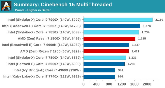
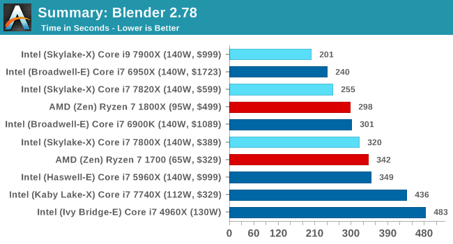
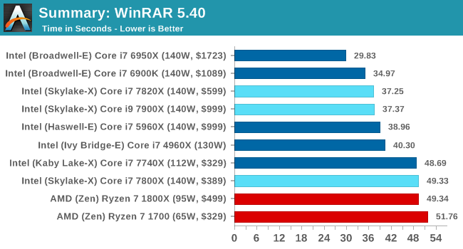
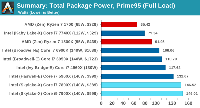
In the end, this is what we get: aside from some tests that are L3 memory sensitive such as DigiCortex, WinRAR, and some of the PCMark8 tests, the Core i9-7900X wins every CPU test. For anyone who was unsure about getting the 10-core on the last generation on a compute basis, this new one seems to be the one to get.
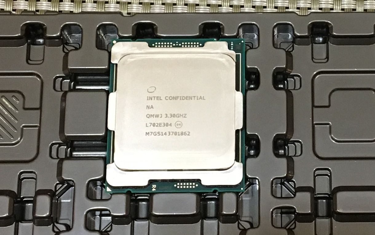
The gaming story is unfortunately not quite as rosy. We had last minute BIOS updates to a number of our boards because some of the gaming tests were super underperforming on the new Skylake-X parts. We are told that these early BIOSes are having power issues to do with turboing, as well as Intel’s Speed Shift technology when the GPU is active.
While these newer BIOSes have improved things, there are still some remaining performance issues to be resolved. Our GTX1080 seems to be hit the hardest out of our four GPUs, as well as Civilization 6, the second Rise of the Tomb Raider test, and Rocket League on all GPUs. As a result, we only posted a minor selection of results, most of which show good parity at 4K. The good news is that most of the issues seem to happen at 1080p, when the CPU is more at fault. The bad news is that when the CPU is pushed into a corner, the current BIOS situation is handicapping Skylake-SP in gaming.
I'm going to hold off on making a final recommendation for gaming for the moment, as right now there are clear platform problems. I have no doubt Intel and the motherboard vendors can fix them – this isn't the first time that we've seen a new platform struggle at launch (nor will it be the last). But with pre-orders opening up today, if you're a gamer you should probably wait for the platform to mature a bit more and for the remaining gaming issues to be fixed before ordering anything.
Itching for 18 Cores?
While today is the launch for Skylake-X CPUs up to 10-cores, a lot of talk will be around the 18-core Core i9-7980XE part due later this year, coming out at $1999. Double the price of the 10-core will unlikely equal double the performance, as we would expect lower frequencies to compensate. But users who need 18 lots of AVX-512 support will be rubbing their hands with glee. It will also be an interesting one to overclock, and I suspect that certain companies are already planning ahead to break some world records with it. We’ll try and get a sample in.
Should I wait for the 12-core? For ThreadRipper? Or Just Go Ryzen?
Both the 12-core Core i9-7920X and AMD’s ThreadRipper parts are set to launch this summer, with the Intel part confirmed in the August timeframe. By this time the X299 ecosystem should be settling down, while AMD will have to navigate a new X399 ecosystem, which I’m getting mixed messages about (some motherboard vendors say they are almost ready, others say they’re not even close). Both of these CPUs will be exchanging more cores for frequency, and the cost is a big factor – we don’t know for how much ThreadRipper or the X399 motherboards will retail for.
Ultimately a user can decide the following:
- To play it safe, invest in the Core i9-7900X today.
- To play it safe and get a big GPU, save $400 and invest in the Core i7-7820X today.
- To play it cheaper but competitive, invest in Ryzen 7 today.
- To invest in PCIe connectivity, wait for ThreadRipper. 60 PCIe lanes are hard to ignore.
- To invest in AVX512, wait for the next Intel CPUs.
So What’s the Takeaway Here?
From an engineering perspective, Intel is doing new things. The cache, the mesh, and AVX512 are interesting changes from several years of iterative enhancements on the prosumer side, but it will take time to see how relevant they will become. For some enterprise applications, they will make perfect sense.
From a consumer/prosumer perspective, it breaks the mold by offering some CPUs now and some CPUs later. The hardware itself won’t feel too much different, aside from having all the Intel cores and software slowly taking advantage. But Intel’s 10-core, at $999, suddenly got easier to recommend for users in that price bracket. At $599 though, the 8-core saves several hundred dollars for other upgrades if you don’t need AVX-512 or 44 PCIe lanes.


